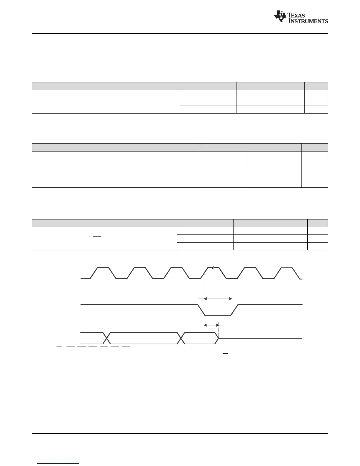
PWM
(B)
TZ
(A)
SYSCLK
t
w(TZ)
t
d(TZ-PWM)HZ
132
TMS320F28069
,
TMS320F28068
,
TMS320F28067
,
TMS320F28066
TMS320F28065, TMS320F28064, TMS320F28063, TMS320F28062
SPRS698F –NOVEMBER 2010–REVISED MARCH 2016
www.ti.com
Submit Documentation Feedback
Product Folder Links: TMS320F28069 TMS320F28068 TMS320F28067 TMS320F28066 TMS320F28065
TMS320F28064 TMS320F28063 TMS320F28062
Detailed Description Copyright © 2010–2016, Texas Instruments Incorporated
6.9.9.1 ePWM Electrical Data/Timing
PWM refers to PWM outputs on ePWM1–8. Table 6-58 shows the PWM timing requirements and Table 6-
59, switching characteristics.
(1) For an explanation of the input qualifier parameters, see Table 6-76.
Table 6-58. ePWM Timing Requirements
(1)
MIN MAX UNIT
t
w(SYCIN)
Sync input pulse width
Asynchronous 2t
c(SCO)
cycles
Synchronous 2t
c(SCO)
cycles
With input qualifier 1t
c(SCO)
+ t
w(IQSW)
cycles
Table 6-59. ePWM Switching Characteristics
over recommended operating conditions (unless otherwise noted)
PARAMETER TEST CONDITIONS MIN MAX UNIT
t
w(PWM)
Pulse duration, PWMx output high/low 33.33 ns
t
w(SYNCOUT)
Sync output pulse width 8t
c(SCO)
cycles
t
d(PWM)tza
Delay time, trip input active to PWM forced high
Delay time, trip input active to PWM forced low
no pin load 25 ns
t
d(TZ-PWM)HZ
Delay time, trip input active to PWM Hi-Z 20 ns
6.9.9.2 Trip-Zone Input Timing
(1) For an explanation of the input qualifier parameters, see Table 6-76.
Table 6-60. Trip-Zone Input Timing Requirements
(1)
MIN MAX UNIT
t
w(TZ)
Pulse duration, TZx input low
Asynchronous 2t
c(TBCLK)
cycles
Synchronous 2t
c(TBCLK)
cycles
With input qualifier 2t
c(TBCLK)
+ t
w(IQSW)
cycles
A. TZ - TZ1, TZ2, TZ3, TZ4, TZ5, TZ6
B. PWM refers to all the PWM pins in the device. The state of the PWM pins after TZ is taken high depends on the PWM
recovery software.
Figure 6-50. PWM Hi-Z Characteristics

 Loading...


