NORA-W10 series - System integration manual
UBX-22005601 - R04 Design-in Page 19 of 56
C1-Public
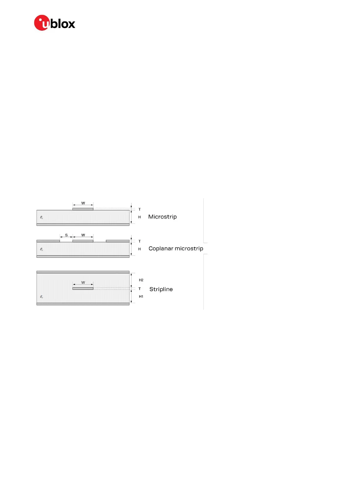
Figure 6 shows the design options for implementing a transmission line, namely:
• Microstrip – track separated with dielectric material and coupled to a single ground plane.
• Coplanar microstrip – track separated with dielectric material and coupled to both the ground plane
and side conductor.
• Stripline – track separated by dielectric material and sandwiched between two parallel ground
planes.
The parameters shown in the cross-sectional area of each trace design include:
• Width (W) – shows the width of the copper layer on the top layer
• Distance (S) – shows the distance between the top copper layer and the two adjacent GND planes.
• Dielectric substrate thickness (H) – shows the distance between the GND reference on the bottom
plane and the copper layer on the top layer.
• Thickness of the copper layer (T) – can also be represented by “Base Copper Weight”, which is
commonly used as the parameter for PCB stack-up.
• Dielectric constant (ε
r
) defines the ratio between the electric permeability of the material against
the electric permeability of free space.
☞ The width of a 50 Ω microstrip depends on “ε
r
” and “H”, which must be calculated for each PCB
layer stack-up.
Figure 6: Transmission line trace design
Follow these recommendations to design a 50 transmission line correctly:
• The designer should provide enough clearance from surrounding traces and ground in the same
layer; in general, a trace to ground clearance of at least two times the trace width should be
considered. The transmission line should also be “guarded” by ground plane area on each side.
• The characteristic impedance can be calculated as first iteration using tools provided by the layout
software. It is advisable to ask the PCB manufacturer to provide the final values that are usually
calculated using dedicated software and available stack-ups from production. It could also be
possible to request an impedance coupon on panel’s side to measure the real impedance of the
traces.
• FR-4 dielectric material, although its high losses at high frequencies can be considered in RF
designs provided that:
 Loading...