MAX-M10M-Integration manual
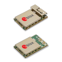
If the hardware backup mode is not used, leave the V_BCKP pin open.
4.1.4 Supply design examples
The two voltage ranges for V_IO allow several combinations when designing the receiver power
supply. Depending on the chosen combination, there are certain requirements to be considered.
These are summarized in Table 30.
Option Nominal supply (V) Design case / Requirements
V_IO VCC
1 3.3 3.3
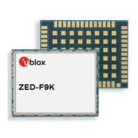
3.3 V design where VCC and V_IO are connected together. See Figure 21 for designs
using the hardware backup mode, and Figure 22 for designs without backup supply.
• VIO_SEL pin left open.
• Voltage at VCC_RF pin = VCC - 0.1 V.
2 1.8 1.8
1.8 V design with VCC and V_IO connected together. This design requires an
accurate supply. See Figure 21 for designs using the hardware backup mode, and
Figure 22 for designs without backup supply.
• VIO_SEL is grounded.
• Note that the voltage output at VCC_RF = VCC - 0.1 V.
• Note that the maximum supply tolerance is 1.8 V ± 2 %.
To enter hardware backup mode, set the receiver to software standby mode
with the UBX-RXM-PMREQ message before switching off V_IO and VCC.
3 1.8 1.8 / 3.3 / 5.0
VCC and V_IO are supplied independently. V_IO is supplied with an accurate 1.8 V
supply. VCC can be either supplied with 1.8 V , 3.3 V or 5.0 V. See Figure 23 for
designs using the hardware backup mode, and Figure 24 for designs without backup
supply.
• VIO_SEL pin is grounded.
• Note that the maximum supply tolerance is 1.8 V ± 2 %.
• Voltage at VCC_RF pin = VCC - 0.1 V.
To enter hardware backup mode, switch off V_IO 100 ms before VCC.
Alternatively, the receiver can be set to software standby mode with the UBX-
RXM-PMREQ message before switching off V_IO and VCC.
Table 30: Voltage supply options
Figure 21: VCC and V_IO connected to the main supply, and external power supply at V_BCKP
Figure 22: VCC and V_IO connected to the main supply. No external power supply at V_BCKP.
UBX-22038241 - R02
4 Hardware integration Page 65 of 92
C1-Public