Doc. No: Unex-QSG-21-003
19/30
A printed version of this document is an uncontrolled copy
© 2023 Unex Technology Corporation – Company Confidential
Switching of internal/external GNSS and 1PPS signal is not controlled by DIP switch.
Please see 9.8 1PPS for detailed instruction.
Table 11: DIP Switch Functions
9. Design-in Guidelines
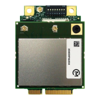
The SOM-352 pinout is compatible with most standard PCIe mini card interfaces.
However, it may need to be fed with 5V DC power and connecting other I/O interfaces
through an external cable when installed on an existing mPCIe system board. A customized
PCIe mini card pinout can help user to get rid of the extra cable and to rely on the PCIe
mini card interface alone. A design-in system board solution may provide improved
reliability, simpler installation, and cost saving to the overall system.
9.1. Power Line Traces
• Power line traces should be as wide as possible, in order to reduce impedance of
these lines.
• Crossing by any other lines of upper or lower layer should also be avoided.
• The maximum power consumption occurs during RF transmission. A typical
transmitting frame lasts 1-2ms.
• It is recommended to keep the 5V supply current no less than 2A (continuous) to
keep RF performance from degradation.
• If the SOM-352 halts or resets while performing a V2X RF transmission, it is
recommended to add a bulk capacitor on the 5V trace near the mPCIe connector to
 Loading...