Doc. No: Unex-QSG-21-003
3/30
A printed version of this document is an uncontrolled copy
© 2023 Unex Technology Corporation – Company Confidential
TABLE OF CONTENTS
1. Objective ................................................................................................... 6
2. Reference ................................................................................................. 6
3. Limited Warranty Policy ............................................................................ 6
4. Safety Guidelines ...................................................................................... 7
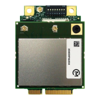
5. Product Appearance ................................................................................. 7
6. Functional Block Diagram ......................................................................... 8
7. Electrical Characteristics .......................................................................... 9
7.1. Absolute Maximum Ratings .................................................................................. 9
7.2. Recommended Operating Conditions ................................................................... 9
7.3. Power Consumption ............................................................................................ 10
8. I/O Interfaces .......................................................................................... 11
8.1. Antenna Connectors ............................................................................................ 11
8.1.1. 5.9GHz V2X .......................................................................................... 13
8.1.2. GNSS .................................................................................................... 14
8.2. Mini PCIe Card Pinout ......................................................................................... 15
8.3. I/O Cable Pinout .................................................................................................. 17
8.4. DIP Switch ........................................................................................................... 18
9. Design-in Guidelines ............................................................................... 19
9.1. Power Line Traces .............................................................................................. 19
9.2. Power Sequence ................................................................................................. 20
9.3. Brown Out ........................................................................................................... 20
9.4. Grounding ........................................................................................................... 20
9.5. USB Data Lines ................................................................................................... 20
9.6. Serial Port ........................................................................................................... 21
9.7. Reset ................................................................................................................... 22
9.8. 1PPS ................................................................................................................... 22
9.9. BOOTSTRP ........................................................................................................ 23
9.10. Tamper Detection (Optional) ............................................................................... 23
9.10.1. Production Mode ................................................................................... 24
9.10.2. Test Mode ............................................................................................. 24
9.11. Thermal Management ......................................................................................... 25
9.12. Firmware Upgrade .............................................................................................. 25
9.12.1. Manual control ...................................................................................... 25
 Loading...