Doc. No: Unex-QSG-21-003
4/30
A printed version of this document is an uncontrolled copy
© 2023 Unex Technology Corporation – Company Confidential
9.12.2. Host GPIO control ................................................................................. 26
10. Dimensions and Weight .......................................................................... 26
10.1. Component Keep Out Area ................................................................................. 27
11. Software Settings .................................................................................... 28
11.1. Verifying the Integration with a Host System ...................................................... 28
11.1.1. Windows 10/11 ...................................................................................... 28
11.1.2. Linux ..................................................................................................... 29
12. Troubleshooting ...................................................................................... 30
12.1. Repetitive Resetting When Using 3.3V Single Voltage Supply .......................... 30
12.2. No Response After Applying Power .................................................................... 30
LIST OF FIGURES
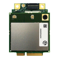
Figure 1: SOM-352 series appearance ..................................................................................... 8
Figure 2: Functional block diagram ........................................................................................... 8
Figure 3: Antenna connectors .................................................................................................. 12
Figure 4: Antenna cable extraction tool ................................................................................... 13
Figure 5: V2X antennas EX-55/EX-53 ..................................................................................... 13
Figure 6: I/O Cable mating component P/N ............................................................................ 18
Figure 7: Onboard DIP switch ................................................................................................. 18
Figure 8: USB data line routing example ................................................................................. 21
Figure 9: External 1PPS input pins.......................................................................................... 23
Figure 10: Thermally conductive pad area .............................................................................. 25
Figure 11: SOM-352 dimensions ............................................................................................. 27
LIST OF TABLES
Table 1. Absolute maximum ratings ........................................................................................... 9
Table 2. Recommended operating conditions ........................................................................... 9
Table 3. Dual voltage power consumption ............................................................................... 10
Table 4. External cable power consumption ............................................................................. 11
Table 5. Single voltage power consumption ............................................................................. 11
Table 6: V2X antenna status .................................................................................................... 13
Table 7: GNSS antenna status ................................................................................................ 15
Table 8: SOM-352 mini PCIe row 0 pinout .............................................................................. 15
Table 9: SOM-352 mini PCIe row 1 pinout .............................................................................. 16
Table 10: I/O cable pinout ........................................................................................................ 17
Table 11: DIP Switch Functions ............................................................................................... 19
Table 12: Dimensions and weight ............................................................................................ 27
Table 13: Unex BSP interface settings .................................................................................... 28
 Loading...