VA41620/VA41630 Evaluation Board User’s Manual
V1.0
3
development tools. The J-Link OB allows the board to be connected directly to the USB port of
a PC to allow:
- Power supplied from the USB 5V source supply
- JTAG communications for debug and programming
- Terminal communications to allow data transfer between a PC terminal window and
the VA416x0 MCU.
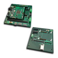
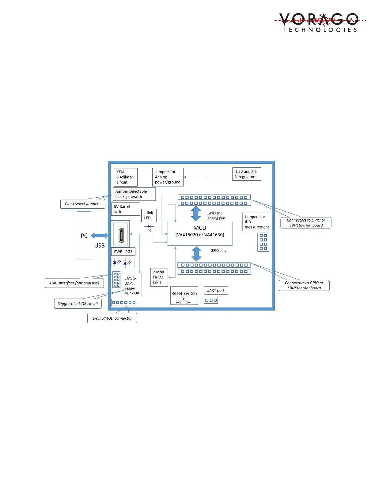
A block diagram of the MCU evaluation board is shown in Figure 1. The MCU evaluation board
conveniently stacks on to resource boards for maximum development flexibility. If compact size
is preferred, the MCU board may be used standalone with full JTAG and includes a UART for
background communication.
Figure 1 - Block diagram of PEB1
1.3.2 The PEB1 GPIO board
The PEB1 GPIO board provides additional connectivity to the VA416x0 MCU. Access to all 104
GPIO pins are available on the various convenient headers. Header pins located on the GPIO
board as well provide access to integrated board resources, ADC inputs, DAC outputs, I2C
interfaces, CAN interfaces with transceivers, and a connector for a SpaceWire interface. An
accelerometer is provided on the board as well, with access via one of the three I2C interfaces.
An external SPI accessible FRAM device is also included on the board. Four PMOD connectors
are available for the I2C, UART, and SPI peripherals.