Alto Hardware Manual
LDA
0
DATA
COM
0 0
LDA
l·DATAMASK
AND
1 0
LDA
3
UTILOUTADR
STA
0 0 3
LDA
1
DATATOGGLE
DIAGNOSE2
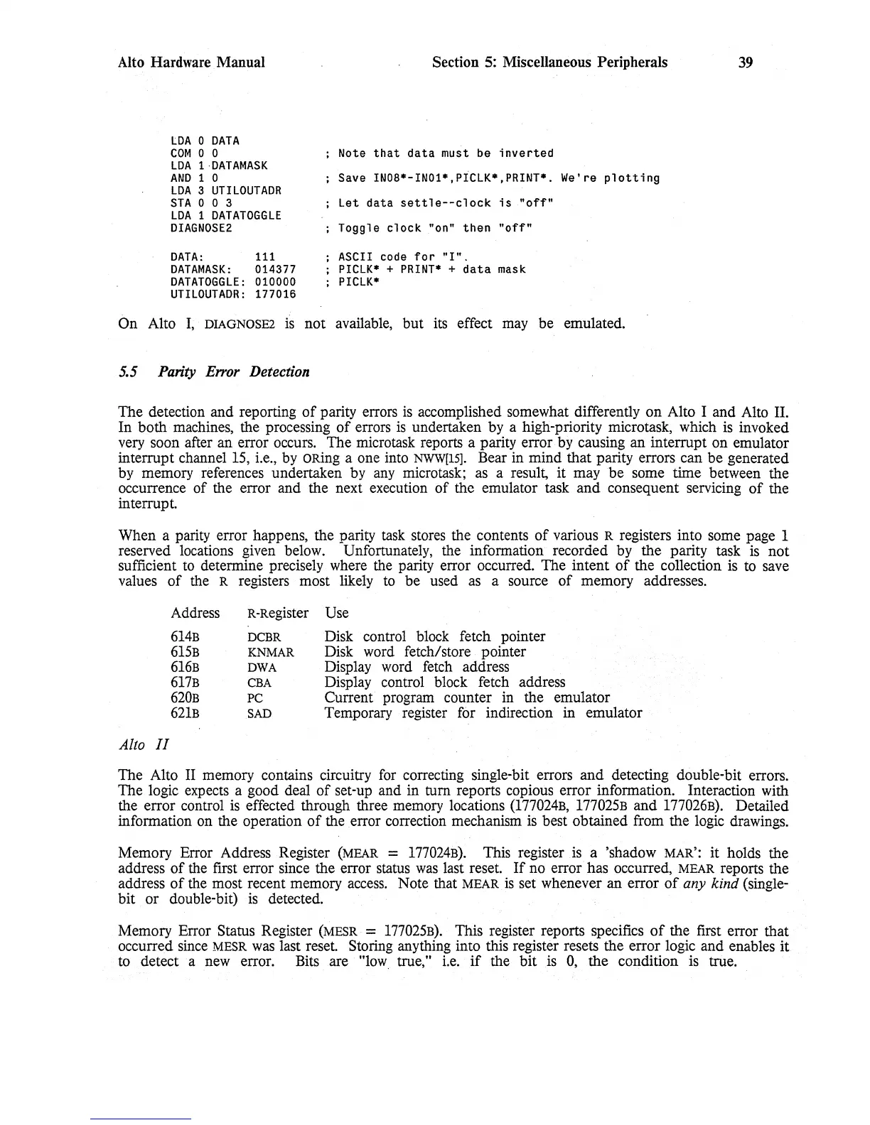
DATA:
111
DATAMASK:
014377
DATATOGGLE:
010000
UTILOUTADR:
177016
Section
5:
Miscellaneous Peripherals
Note
that
data
must be
inverted
Save IN08*-IN01*,picLK*,PRINT*. We're
plotting
Let
data
settle--clock
is
"off"
Toggle
clock
"on"
then
"off"
ASCII
code
for
"I".
PICLK*
+
PRINT*
+
data
mask
PICLK*
On Alto
I;
DIAGNOSE2
is
not available, but its effect
may
be emulated.
5.5
Parity
Error
Detection
39
The detection and reporting
of
parity errors
is
accomplished somewhat differently on Alto I and
Alto
II.
In both machines, the processing
of
errors
is
undertaken
by
a high-priority microtask, which
is
invoked
very
soon after an error occurs. The microtask reports a parity error
by
causing an interrupt on emulator
interrupt channel
15,
i.e.,
by
ORing
a one into
NWW[15j.
Bear in mind that parity errors can be generated
by
memory references undertaken
by
any
microtask;
as
a result, it may be some time between the
occurrence of the error and the next execution
of
the emulator task and consequent servicing
of
the
interrupt
When a parity error happens, the parity
task
stores the contents
of
various R registers into some page 1
reserved locations given below. Unfortunately, the information recorded
by
the parity task
is
not
sufficient
to
determine precisely where
the
parity error occurred. The intent
of
the collection
is
to
save
values
of
the R registers most likely
to
be used
as
a source
of
memory addresses.
Alto
II
Address
614B
615B
616B
617B
620B
621B
R-Register
DCBR
KNMAR
DWA
CBA
PC
SAD
Use
Disk control block fetch pointer
Disk word fetch/store pointer
Display
word
fetch
address
Display control block fetch address
Current program counter
in
the emulator
Temporary register
for
indirection in emulator
The Alto
II
memory contains circuitry
for
correcting single-bit errors and detecting double-bit errors.
The logic
expects
a good deal
of
set-up and in turn reports copious error information. Interaction with
the error control
is
effected through three memory locations
(177024B,
177025B
and
177026B).
Detailed
information on the operation
of
the error correction mechanism
is
best obtained from the
logic
drawings.
Memory Error Address Register
(MEAR
=
177024B).
This register
is
a 'shadow
MAR':
it holds the
address
of
the first error since the error status
was
last reset.
If
no error has occurred,
MEAR
reports the
address
of
the most recent memory
access.
Note that
MEAR
is
set whenever an error
of
any kind (single-
bit or double-bit)
is
detected.
Memory Error Status Register
(MESR
=
177025B).
This register reports specifics
of
the first error that
occurred
since
MESR
was
last reset. Storing anything into this register resets the error logic and enables it
to
detect a
new
error.
Bits
are "low true,"
i.e.
if
the bit
is
0,
the condition
is
true.
 Loading...