ML505/ML506/ML507 Getting Started Tutorial www.xilinx.com 27
UG348 (v3.0.2) October 9, 2008
ML50x Demonstrations in Linear Flash
R
impact -batch etc/download.cmd
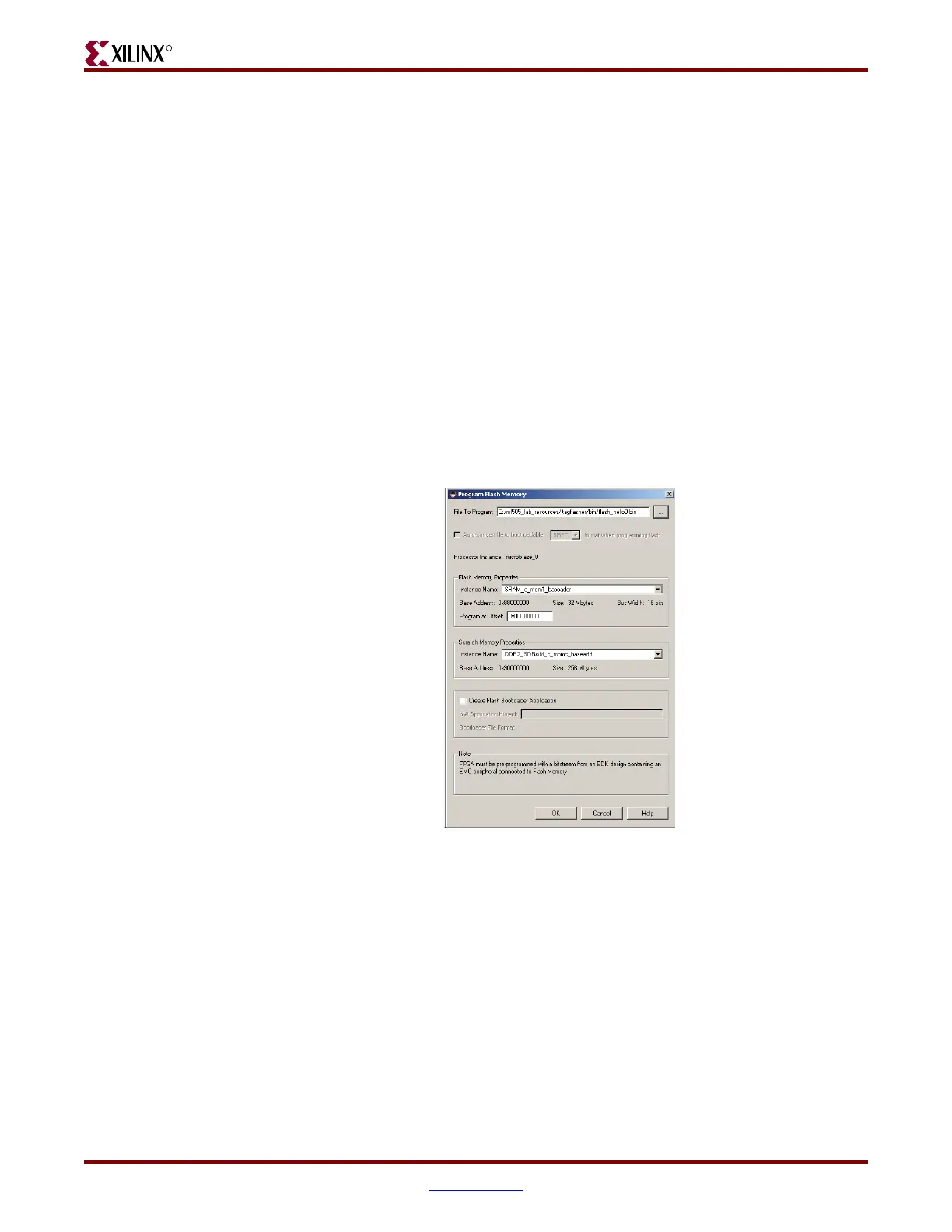
7. Program the linear flash at a specific configuration location (Figure 12). From the EDK
GUI menu, select Device Configuration → Program Flash Memory
Enter the path of the flash image:
<LAB_DIR>/flash_hello0.bin
Set the Flash Memory Properties, Instance Name to SRAM_c_mem1_baseaddr
Set the Flash Memory Properties, Program at Offset as follows:
For Configuration 0, set the address to 0x00000000
For Configuration 1, set the address to 0x00800000
For Configuration 2, set the address to 0x01000000
For Configuration 3, set the address to 0x01800000
Set the Scratch Memory Properties, Instance Name to
DDR2_SDRAM_c_mpmc_baseaddr
Click OK. Repeat this step for each BIN file to be programmed into the linear flash.
8. Select and set the CONFIG DIP switch values to indicate the desired linear flash
configuration location:
Configuration 0: 00001001
Configuration 1: 00101001
Configuration 2: 01001001
Configuration 3: 01101001
9. Press the PROG pushbutton to configure the Virtex-5 FPGA from the linear flash
using the configuration selected in step 8.
Figure 12: Programming the Flash
UG348_10_120108

 Loading...


