ML605 Hardware User Guide www.xilinx.com 19
UG534 (v1.2.1) January 21, 2010
Detailed Description
The Memory Interface Generator (MIG) tool guidelines specify a set of U1 FPGA “No
Connect” pins. These should be added to the UCF as CONFIG PROHIBIT pins as follows:
CONFIG PROHIBIT = H22;
CONFIG PROHIBIT = F21;
CONFIG PROHIBIT = B20;
CONFIG PROHIBIT = F19;
CONFIG PROHIBIT = C13;
CONFIG PROHIBIT = M12;
CONFIG PROHIBIT = L13;
CONFIG PROHIBIT = K14;
CONFIG PROHIBIT = F25;
CONFIG PROHIBIT = C29;
CONFIG PROHIBIT = C28;
CONFIG PROHIBIT = D24;
References
See the Micron Technology, Inc. for more information [Ref 22].
In addition, see the Virtex-6 FPGA Memory Interface Solutions User Guide [Ref 6] and the
Virtex-6 FPGA Memory Resources User Guide [Ref 9].
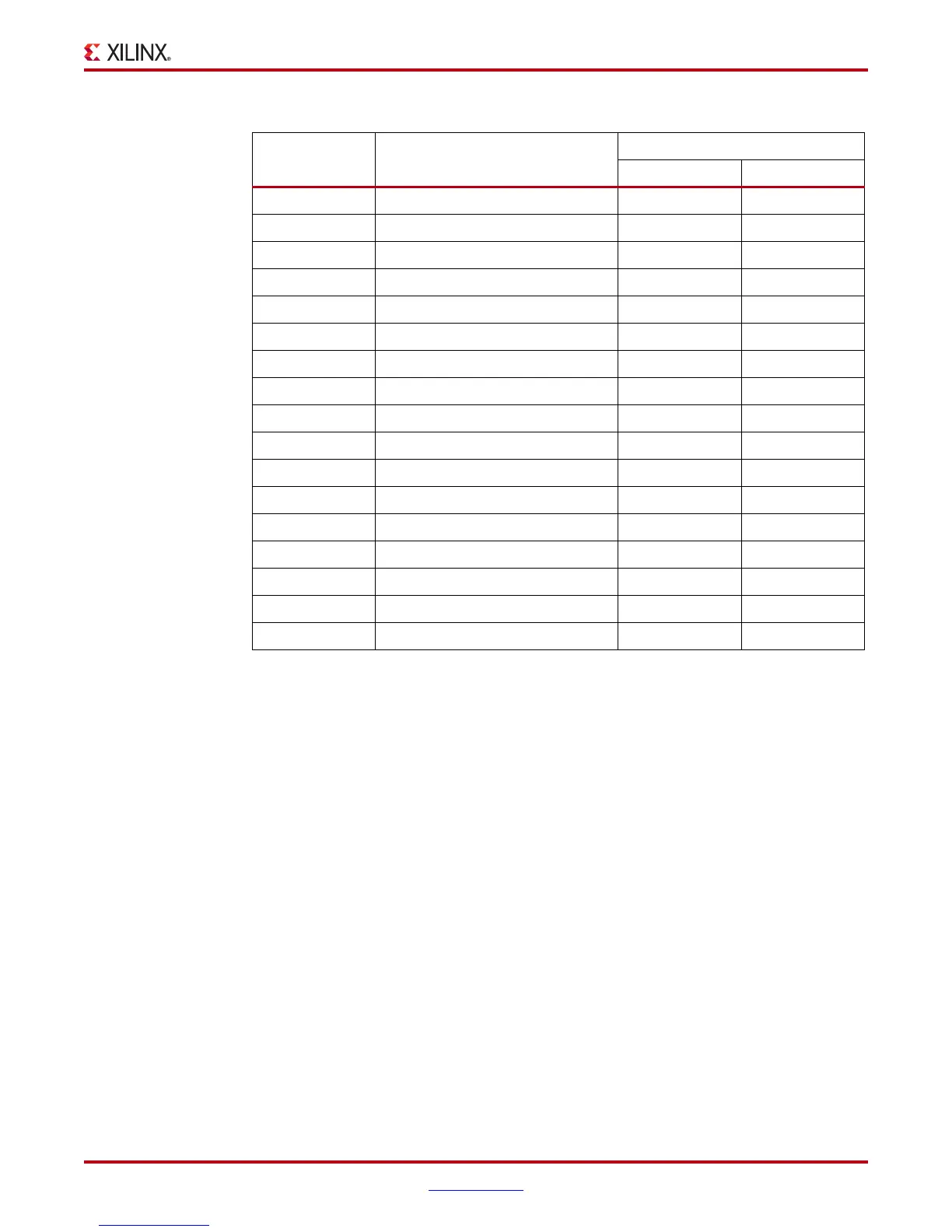
C30 DDR3_DQS7_P 188 DQS7_P
F18 DDR3_ODT0 116 ODT0
E17 DDR3_ODT1 120 ODT1
E18 DDR3_RESET_B 30 RESET_B
K18 DDR3_S0_B 114 S0_B
K17 DDR3_S1_B 121 S1_B
D17 DDR3_TEMP_EVENT 198 EVENT_B
B17 DDR3_WE_B 113 WE_B
C17 DDR3_CAS_B 115 CAS_B
L19 DDR3_RAS_B 110 RAS_B
M18 DDR3_CKE0 73 CKE0
M17 DDR3_CKE1 74 CKE1
H18 DDR3_CLK0_N 103 CK0_N
G18 DDR3_CLK0_P 101 CK0_P
L16 DDR3_CLK1_N 104 CK1_N
K16 DDR3_CLK1_P 102 CK1_P
Table 1-4: DDR3 SODIMM Connections (Cont’d)
U1 FPGA Pin Schematic Net Name
J1 SODIMM
Pin Number Pin Name