VC7203 IBERT Getting Started Guide www.xilinx.com 9
UG847 (v4.0) November 6, 2013
Running the GTX IBERT Demonstration
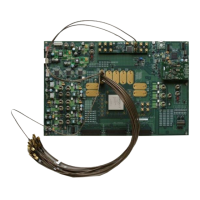
All GTX transceiver pins and reference clock pins are routed from the FPGA to a connector
pad which interfaces with Samtec BullsEye connectors. Figure 1-2 A shows the connector
pad. Figure 1-2 B shows the connector pinout.
The SuperClock-2 module provides LVDS clock outputs for the GTX transceiver reference
clocks in the IBERT demonstrations. Figure 1-3 shows the locations of the differential clock
SMA connectors on the clock module which can be connected to the reference clock cables.
Note:
The image in Figure 1-3 is for reference only and might not reflect the current revision of the
board.
The four SMA pairs labeled CLKOUT provide LVDS clock outputs from the Si5368 clock
multiplier/jitter attenuator device on the clock module. The SMA pair labeled Si570_CLK
provides LVDS clock output from the Si570 programmable oscillator on the clock module.
Note:
The Si570 oscillator does not support LVDS output on the Rev B and earlier revisions of the
SuperClock-2 module.
For the GTX IBERT demonstration, the output clock frequencies are preset to 156.25 MHz.
For more information regarding the SuperClock-2 module, see HW-CLK-101-SCLK2
SuperClock-2 Module User Guide (UG770).
X-Ref Target - Figure 1-2
Figure 1-2: A – GTX Connector Pad. B – GTX Connector Pinout
X-Ref Target - Figure 1-3
Figure 1-3: SuperClock-2 Module Output Clock SMA Locations
8*BFBB
%
*7;
*7;&RQQHFWRU3LQRXW
3
3
3
3
3
3
3
3
3
3
1
1
1
1
1
1
1
1
1
1
5;
7;
7;
5;
7;
&/.
5;
7;
&/.
5;
$
*7;&RQQHFWRU3DG
8*BFBB
&/.287B1
&/.287B1
6,B&/.B1
6,B&/.B3
&/.287B3
&/.287B1 &/.287B1
&/.287B3 &/.287B3 &/.287B3

 Loading...