EasyManuals Logo

Xilinx Virtex-7 FPGA VC7203 User Manual

Xilinx Virtex-7 FPGA VC7203
46 pages
To Next Page IconTo Next Page
To Previous Page IconTo Previous Page
Page #8 background imageLoading...
Page #8 background image
8 www.xilinx.com VC7203 IBERT Getting Started Guide
UG847 (v3.0) July 10, 2013
Chapter 1: VC7203 IBERT Getting Started Guide
All GTX transceiver pins and reference clock pins are routed from the FPGA to a connector
pad which interfaces with Samtec BullsEye connectors. Figure 1-2 A shows the connector
pad. Figure 1-2 B shows the connector pinout.
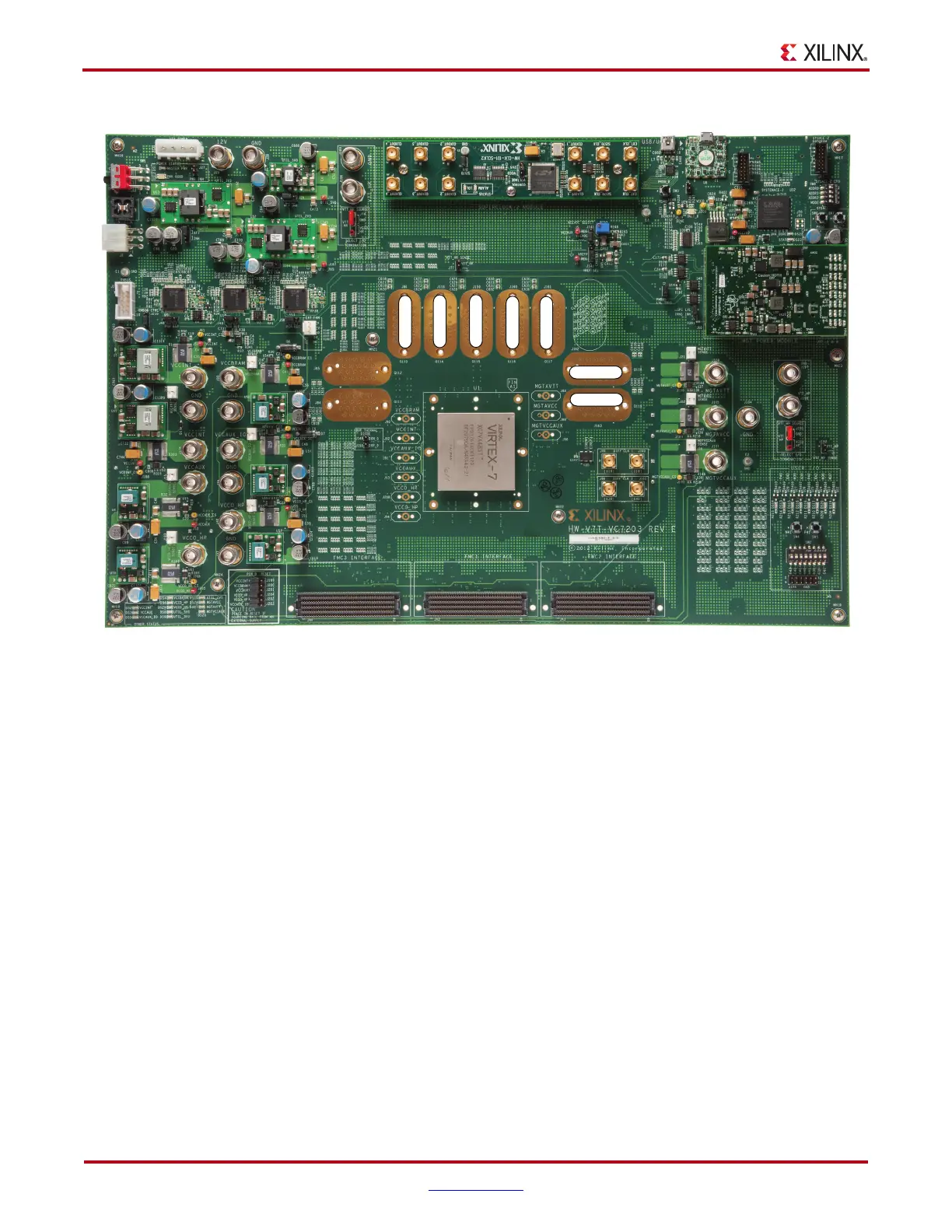
X-Ref Target - Figure 1-1
Figure 1-1: GTX Quad Locations
UG847_c1_01_1026112
QUAD_113
QUAD_114
QUAD_115
QUAD_116
QUAD_117
QUAD_118
QUAD_119

Questions and Answers:

Question and Answer IconNeed help?

Do you have a question about the Xilinx Virtex-7 FPGA VC7203 and is the answer not in the manual?

Xilinx Virtex-7 FPGA VC7203 Specifications

General IconGeneral
FPGA FamilyVirtex-7
DeviceXC7VX485T
Transceivers16
Maximum Transceiver Speed12.5 Gbps
Transceiver TypeGTX
DSP Slices2, 800
Block RAM37, 080 KB
Clock Management Tiles12
PCIe Gen2/Gen3 SupportYes
PackageFFG1761

Related product manuals