VC7203 IBERT Getting Started Guide www.xilinx.com 9
UG847 (v3.0) July 10, 2013
Running the GTX IBERT Demonstration
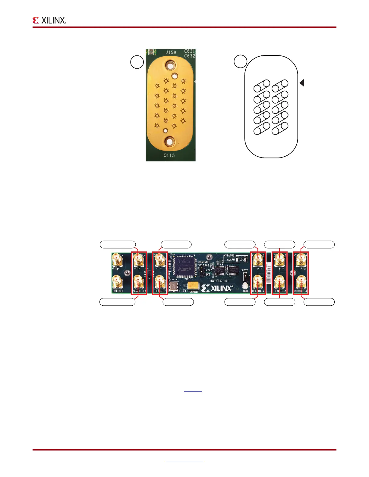
The SuperClock-2 module provides LVDS clock outputs for the GTX transceiver reference
clocks in the IBERT demonstrations. Figure 1-3 shows the locations of the differential clock
SMA connectors on the clock module which can be connected to the reference clock cables.
Note:
The image in Figure 1-3 is for reference only and might not reflect the current revision of the
board.
The four SMA pairs labeled CLKOUT provide LVDS clock outputs from the Si5368 clock
multiplier/jitter attenuator device on the clock module. The SMA pair labeled Si570_CLK
provides LVDS clock output from the Si570 programmable oscillator on the clock module.
Note:
The Si570 oscillator does not support LVDS output on the Rev B and earlier revisions of the
SuperClock-2 module.
For the GTX IBERT demonstration, the output clock frequencies are preset to 156.25 MHz.
For more information regarding the SuperClock-2 module, see HW-CLK-101-SCLK2
SuperClock-2 Module User Guide (UG770
).
Attach the GTX Quad Connector
Before connecting the BullsEye cable assembly to the board, firmly secure the blue
elastomer seal provided with the cable assembly to the bottom of the connector housing if
X-Ref Target - Figure 1-2
Figure 1-2: A – GTX Connector Pad. B – GTX Connector Pinout
X-Ref Target - Figure 1-3
Figure 1-3: SuperClock-2 Module Output Clock SMA Locations
UG847_c1_02_110112
B
GTX
GTX Connector Pinout
P
P
P
P
P
P
P
P
P
P
N
N
N
N
N
N
N
N
N
N
RX1
TX1
TX2
RX2
TX0
CLK1
RX3
TX3
CLK0
RX0
A
GTX Connector Pad
UG847_c1_03_103112
CLKOUT3_N
CLKOUT1_N
SI570_CLK_N
SI570_CLK_P
CLKOUT1_P
CLKOUT2_N CLKOUT4_N
CLKOUT2_P CLKOUT3_P CLKOUT4_P

 Loading...
