ZC702 and ZVIK Getting Started Guide www.xilinx.com 15
UG926 (v3.0.1) February 12, 2013
Default Jumper and Switch Settings
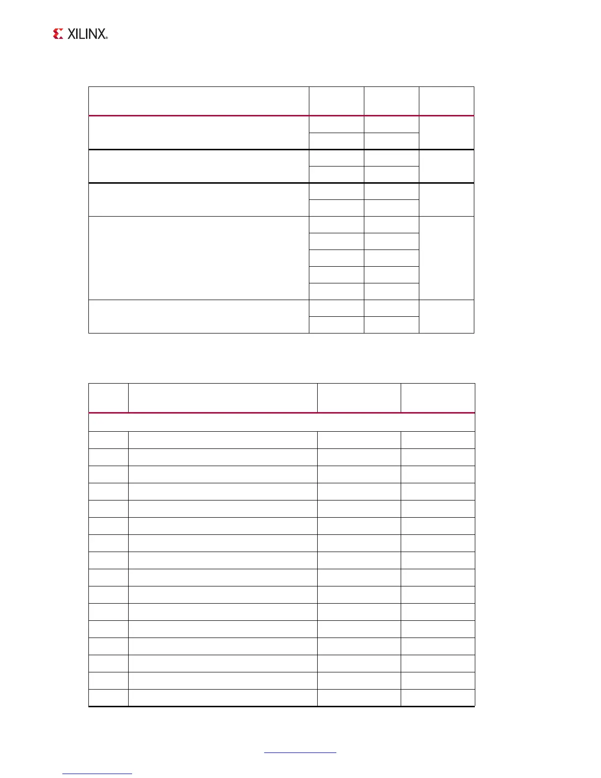
Default jumper positions are shown in Figure 1-4 and listed in Ta ble 1-2.
Table 1-1: Default Switch Settings
Switch Position Setting
Figure 1-4
Callout
SW10
(JTAG chain input select two-position DIP switch)
1Off
9
2On
SW12
(two-position DIP switch)
1Off
2
2Off
SW15
(two-position DIP switch)
1Off
2
2Off
SW16
(five-position DIP switch)
1Right
1
2Right
3Right
4Right
5Right
SW11
(power slide switch)
Off
8
1Down
Table 1-2: Default Jumper Settings
Jumper Function Default Position
Figure 1-4
Callout
HDR_1 X 2
J5 CFGBVS short to GND
OFF 4
J6 POR Master Reset
OFF 1
J7 USB 2.0 USB_VBUS_SEL
ON 6
J8 XADC GND L3 Bypass
OFF 2
J9 XADC GND
ON 2
J10 ARM HDR J41 pin 2 to VADJ
OFF 7
J11 UCD9248 U32 ADDR52 RESET_B
OFF 4
J12 FMC_VADJ_ON_B
ON 4
J13 UCD9248 U33 ADDR53 RESET_B
OFF 3
J14 UCD9248 U34 ADDR54 RESET_B
OFF 5
J15 CAN BUS COMMON-MODE CANH HDR
ON 7
J43 Ethernet PHY HDR
ON 7
J44 USB 2.0 USB_RESET_B
OFF 7
J53 CAN BUS COMMON-MODE CANL HDR
ON 7
J56 JTAG HDR J58 pin 2 3.3V SEL
OFF 9
J65 XADC_VCC5V0 = VCC5V0
ON 2

 Loading...


