7
Circuit Description
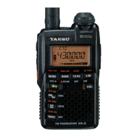
The VX-7R consists of a RF-UNIT, a CNTL-UNIT and
an AF-UNIT. The RF-UNIT contains the receiver front
end, PLL IC, power and switching circuits, and the VCO-
UNIT for transmit and receive local signal oscillation.
The CNTL-UNIT contains the CPU, and audio ICs, and
the power circuitry for the LCD. The AF-UNIT contains
the IF, and audio ICs.
Receiver Signal Flow
The VX-7R includes five receiver front ends, each
optimized for a particular frequency range and mode
combination.
(1) Triplexer
Signals between 0.5 and 540 MHz received at the an-
tenna terminal pass through a first low-pass filter com-
posed of C1266, C1269, C1289, C1291, C1296, C1297,
L1059, L1060, L1067 and L1068.
Received 430-MHz signals, after passing through the
low-pass filter, are fed to the UHF T/R switch circuit com-
posed of diode switch D1048 (RLS135), D1051 (1SV307).
Received 145-MHz signals, after passing through the
low-pass filter, are fed to the VHF T/R switch circuit com-
posed of diode switch D1053 (RLS135), D1054 (1SV307).
Received 50-MHz signals, after passing through the
low-pass filter, are fed to the 50MHz T/R switch circuit
composed of diode switch D1058 (RLS135), D1059
(1SV307).
(2) 145-MHz Band and 76-300MHz Reception
Received signals between 76 and 300 MHz pass through
the Triplexer circuit, low-pass filter/high-pass filter cir-
cuit, VHF T/R switch circuit and protector diode D1002
(1SS362) before additional filtering by a band-pass fil-
ter prior to application to RF amplifier Q1004 (2SC5555).
The amplified RF signal is passed through a band-pass
filter to first mixer Q1012 (2SC5555). Meanwhile, VHF
output from the VCO-UNIT is amplified by Q1017
(2SC5374) and applied through diode T/R switch D1041
(DAN222) to mixer Q1012 as the first local signal.
The 47.25-MHz intermediate frequency product of the
mixer is delivered to the AF-UNIT.
The TUNE voltage from the CPU on the CNTL-UNIT
is amplified by DC amplifier Q3017 (NJU7007F2) and
applied to varactors D1020 and D1022 (HVC369B),
D1019, D1021, D1023, D1024, D1033 and D1036 (1SV325)
in the variable frequency band-pass filters. By changing
the electrostatic capacitance of the varactors, optimum
filter characteristics are provided for each specific oper-
ating frequency.
(3) 435-MHz Band and 222-540MHz Reception
Received signals between 222 and 540 MHz pass
through the Triplexer circuit, low-pass filter/high-pass
filter circuit, UHF T/R switch circuit and protector di-
ode D1001 (1SS362) before additional filtering by a band-
pass filter prior to application to RF amplifier Q1003
(2SC5555). The amplified RF signal is passed through a
band-pass filter, RF amplifier Q1006 (2SC5555) and
band-pass filter to first mixer Q1011 (2SC5555). Mean-
while, UHF output from the VCO-UNIT is amplified by
Q1016 (2SC5374) and applied through diode T/R switch
D1045 (HN2D01FU) to mixer Q1011 as the first local sig-
nal.
The 47.25-MHz intermediate frequency product of the
mixer is delivered to the AF-UNIT.
The TUNE voltage from the CPU on the CNTL-UNIT
is amplified by DC amplifier Q3017 and applied to var-
actors D1005, D1018, D1030 and D1031 (HVC358B) in
the variable frequency band-pass filters. By changing the
electrostatic capacitance of the varactors, optimum fil-
ter characteristics are provided for each specific operat-
ing frequency.
(4) 50-MHz-Band and 30-76 MHz Reception
Received signals between 30 and 76 MHz pass through
the Triplexer circuit, low-pass filter circuit, 50 MHz T/R
switch circuit and protector diode D1003 (1SS362) be-
fore additional filtering by a band-pass filter prior to
application to RF amplifier Q1005 (2SC5555). The am-
plified RF signal is passed through a band-pass filter to
first mixer Q1008 (2SC5555). Meanwhile, 50 MHz out-
put from the VCO-UNIT is amplified by Q1018
(2SC5374) and applied through diode T/R switch D1046
(HN2D01FU) to mixer Q1008 as the first local signal.
The 47.25-MHz intermediate frequency product of the
mixer is delivered to the AF-UNIT.
The TUNE voltage from the CPU on the CNTL-UNIT
is amplified by DC amplifier Q3017 and applied to var-
actors D1025 and D1026 (1SV325) in the variable frequen-
cy band-pass filters. By changing the electrostatic capac-
itance of the varactors, optimum filter characteristics are
provided for each specific operating frequency.
 Loading...
