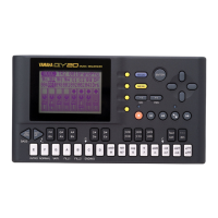
EasyManua.ls Logo

Yamaha A5000 - Page 15

Yamaha A5000
61 pages
Print Icon
To Next Page IconTo Next Page
To Previous Page IconTo Previous Page
Loading...
A5000/A4000
15
MB87034PF (XK851A00) SPC (SCSI Protocol Controller)
PIN
NO.
NAME I/O
FUNCTION
PIN
NO.
NAME I/O
FUNCTION
1
/RESET I
Reset 41
/CLK I
Clock
2
VSS -
Ground 42
VSS -
Ground
3
NC -
43
NC -
4
NC -
44
NC -
5
NC -
45
NC -
6
/DBP I/O
SCSI data bus 46
/I/O I/O
Data direction
7
VSS -
Ground 47
VSS -
Ground
8
/DB7 I/O
48
/REQ I/O
Request
9
/DB6 I/O
SCSI data bus 49
/C/D I/O
Command/Data
10
/DB5 I/O
50
/SEL I/O
Select
11
VDD -
Power supply 51
VDD -
Power supply
12
VSS -
Ground 52
VSS -
Ground
13
VSS -
53
VSS -
14
/DB4 I/O
54
/MSG I/O
Message
15
/DB3 I/O
SCSI data bus 55
/RST I/O
Reset
16
/DB2 I/O
56
/ACK I/O
Acknowledge for REQ
17
/DB1 I/O
57
/BSY I/O
Busy
18
VSS -
Ground 58
VSS -
Ground
19
/DB0 I/O
SCSI data bus 59
/ATN I/O
Attention condition
20
NC -
60
NC -
21
NC -
61
NC -
22
TEST -
62
INT2 O
Non-maskable interrupt request
23
VSS -
Ground 63
VSS -
Ground
24
DRESP I
Response signal for DREQ 64
/CS I
Chip select
25
DREQ O
Data transfer request 65
/WT I
Write strobe
26
HIN I
Output control of HDB0-7,HDBP
66
/WTG I
Data bus write control (to HDB0-7,HDBP)
27
HDB0 I/O
67
/RD I
Read strobe
28
HDB1 I/O
68
/RDG I
Output control for D0-7,DP
29
HDB2 I/O
Data bus 69
D0 I/O
30
HDB3 I/O
(MB87034 <
-
>data memory) 70
D1 I/O
Data bus
31
HDB4 I/O
71
D2 I/O
(MB87034 <
-
>internal register)
32
HDB5 I/O
72
D3 I/O
33
VDD -
Power supply 73
VDD -
Power supply
34
HDB6 I/O
74
D4 I/O
35
HDB7 I/O
Data bus 75
D5 I/O
36
HDBP I/O
76
D6 I/O
Data bus
37
A0 I
77
D7 I/O
38
A1 I
Resistor select 78
DP I/O
39
A2 I
79
DP0 O
Odd number parity of data bus
40
A3 I
80
INTR O
Interrupt request
(IC52)
(IC805)
PCM1716E (XU829A00) DAC (Digital to Analog Converter)
PIN
NO.
NAME
I/O
PIN
NO.
NAME
I/O
FUNCTION
1
LRCK I
15
Vcc1 -
Analog power supply (+5V)
2
DATA I
Data input 16
VOUTL O
Lch, analog voltage output
3
BCK I
Bit clock 17
NC -
4
CLKO O
Clock input 18
EXTL O
Lch, analog output
5
XTI I
Clock input 19
AGND2L -
Analog ground
6
XTO O
Clock out 20
Vcc2L -
Analog power supply (+5V)
7
DGND -
Digital ground 21
/ZERO O
Zero data flag
8
VDD -
Digital power supply (+5V) 22
/RST I
Reset
9
Vcc2R -
Analog power supply (+5V) 23
/CS/IWO I
Chip select
10
AGND2R -
Analog ground 24
MODE I
Mode control select
(H: Software, L: Hardware)
11
EXTR O
Rch, analog output 25
/MUTE I
Mute control
12
NC -
26
MD/DM0 I
Mode control data/ De-emphasis select1
13
14
VOUTR
AGND1
O
-
Rch, analog voltage output
Analog ground
27
28
MC/DM1
ML/IIS
I
I
Mode control BCK/ De-emphasis select2
Mode control Latch/ input format select

Related product manuals