Do you have a question about the Yamaha MG32/14FX and is the answer not in the manual?
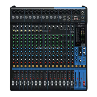
| Type | Analog Mixer |
|---|---|
| Channels | 32 |
| Aux Sends | 6 |
| Line Inputs | 32 |
| Buses | 4 |
| Phantom Power | +48V |
| Outputs | Stereo, Group, Aux, Monitor |
| Mic Inputs | 24 |
| Effects | 2 built-in SPX digital effects processors |
Notice regarding lead in solder and chemicals in components.
Instructions for connecting the mains plug and cord for UK use.
Warning to replace special components with parts of equal specification.
General technical specifications for the mixing console.
Detailed specifications for input and output connectors and levels.
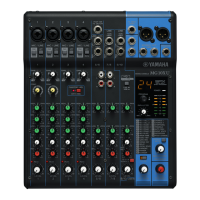
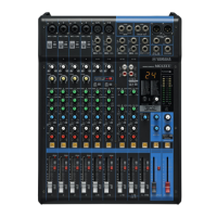
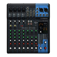
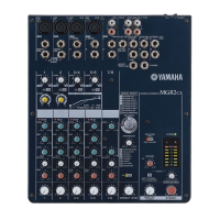
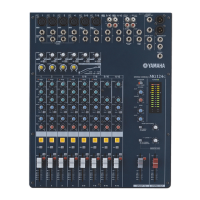
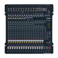
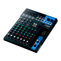
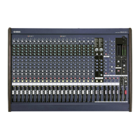
Description of the channel control section on the front panel.
Description of the master control section on the front panel.
Overview of input and output connectors on the rear panel.
Detailed layout and controls for stereo channels.
Layout and controls for group output sections.
Layout and controls for return signal sections.
Description of the 2-track input controls.
Description of the LAMP jack connection.
Details of channel input and output connectors.
Procedure for removing the side pads and flat washers.
Procedure for removing the bottom cover and its screws.
Procedure for removing the left and right side covers.
How to set supports to prevent circuit board distortion.
Steps to remove the PS circuit board and heat sink.
Procedure for removing the power transformer assembly.
Steps to remove the DSP circuit board and shield case.
Procedure for removing the DSP shield base and trans base.
Steps to remove push switches and AC-IN connectors.
Steps for removing the AC inlet connector.
Procedure for removing INJK circuit boards 1 and 2.
Steps to remove the MASJK circuit board.
Procedure for removing IN circuit boards 1, 2, and 3.
Detailed steps for removing IN circuit board 2.
Procedure for removing MAS circuit boards 2/4, 3/4, and 4/4.
Procedure for removing the side pads and flat washers.
Procedure for removing the bottom cover and its screws.
Procedure for removing the left and right side covers.
How to set supports to prevent circuit board distortion.
Steps to remove the PS circuit board and heat sink.
Procedure for removing the power transformer assembly.
Steps to remove the DSP circuit board and shield case.
Procedure for removing the DSP shield base and trans base.
Steps to remove push switches and AC-IN connectors.
Steps for removing the AC inlet connector.
Procedure for removing INJK circuit boards 1, 2, and 3.
Steps to remove the MASJK circuit board.
Procedure for removing IN circuit boards 1, 2, and 3.
Procedure for removing MAS circuit boards 2/4, 3/4, and 4/4.
Pin description for the M30622MCA-1M3FP MCU.
Pin description for the YSS910-S DSP6.
Pin description for the YM3436DK DIR2.
Pin description for the AK4522VF-E2 CODEC.
Block diagram for the 74HCU04DT Hex Inverter IC.
Block diagram for the 74HC08DT Quad 2 Input AND IC.
Block diagram for the NJM4558M Dual Operational Amplifier IC.
Block diagram for the NJM2068MD-T1 IC.
Block diagram for the NJM4580ED Dual Operational Amplifier IC.
Block diagram for the NJM4556AL Dual Operational Amplifier IC.
Block diagram for the LB1412M LED Driver IC.
Diagram showing the component layout of the DSP circuit board.
Diagram showing the component layout of the INJK circuit board.
Diagram showing the component layout of the IN circuit board.
Diagram showing the component layout of the MAS 1/4 circuit board.
Diagram showing the component layout of the MAS 2/4 circuit board.
Diagram showing the component layout of the MAS 3/4 circuit board.
Diagram showing the component layout of the MAS 4/4 circuit board.
Diagram showing the component layout of the MASJK circuit board.
Diagram showing the component layout of the PS circuit board.
Defines the scope of the inspection specifications.
Instructions for using the correct power supply cord.
Procedure for checking power indicators and initializing digital effects.
Procedures for inspecting mixer section functionality.
Preparation steps for mixer section inspection, including load resistance.
Pin description for the M30622MCA-1M3FP MCU.
Pin description for the YSS910-S DSP6.
Pin description for the YM3436DK DIR2.
Pin description for the AK4522VF-E2 CODEC.
Block diagram for the 74HCU04DT Hex Inverter IC.
Block diagram for the 74HC08DT Quad 2 Input AND IC.
Block diagram for the NJM4558M Dual Operational Amplifier IC.
Block diagram for the NJM2068MD-T1 IC.
Block diagram for the NJM4580ED Dual Operational Amplifier IC.
Block diagram for the NJM4556AL Dual Operational Amplifier IC.
Block diagram for the LB1412M LED Driver IC.
List of abbreviations used for model destinations.
Notes on part numbers, interchangeability, and special characteristics.