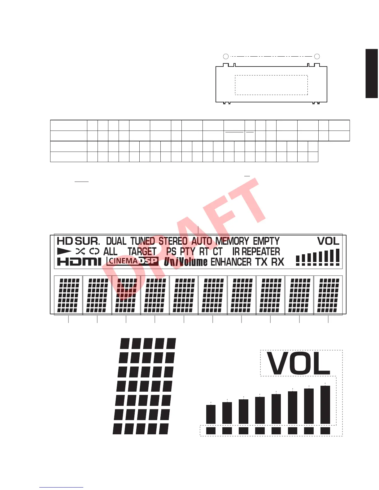
■ DISPLAY DATA
Pin No.
22
NC
21
NC
20
NC
19
NC
18
NC
17
NC
16
NC
15
NC
14
NC
13
NC
12
NC
11
NC
10
NC
9
NC
8
NC
7
NC
6
NC
5
NC
4
NP
3
NP
2
NX
1
F1
Connection
Pin No.
Note: 1) F1, F2 ..... Filament pin 2) NP ..... No pin 3) DL ..... Datum line pin 4) 11G ..... Grid 5) NX ..... No extend pin
6) LGND ..... Logic GND pin 7) PGND ..... Power GND pin 8) VH ..... High voltage supply pin 9) VDD ..... Logic voltage supply pin
10) CP ..... Shift resister clock 11) DA ..... Serial data input 12) TSA, B ..... Test pin 13) CS ..... Chip select input pin
14) RESET ..... Reset input 15) OSC ..... Pin for self-oscillation 16) Q11G ..... Driver output port 17) Solder composition is Sn-3Ag-0.5Cu.
18) NC ..... No connection
Connection
● PIN CONNECTION
● GRID ASSIGNMENT
1
39
● V901 : 011BT267GINAK (POWER P.C.B.)
PATTERN AREA
39 33 32 3138 37 36 35 34 30
F2 VH
29
CS
28
CP
27
DA
24
11GVDD OSC
26
TSA
23
Q11G
25
TSBNX NP NP LGND PGND RESET
11G
1G 2G 3G 4G 5G 6G 7G 8G 9G 10G
(11G)(1G – 10G)
S1
S2
S3
S4
S5
S6
S7
S8
1-1 2-1 3-1 4-1 5-1
1-2 2-2 3-2 4-2 5-2
1-3 2-3 3-3 4-3 5-3
1-4 2-4 3-4 4-4 5-4
1-5 2-5 3-5 4-5 5-5
1-6 2-6 3-6 4-6 5-6
1-7 2-7 3-7 4-7 5-7
S9
81
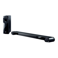
YSP-CU4300/YSP-CU3300/NS-WSW160
YSP-CU4300/YSP-CU3300/
NS-WSW160