SR23 - 923-03509 3-3 CS - SERVICING
CIRCUIT OVERVIEW (continued)
J2402
91-2053
R2936M
100
C2408M
1000pF 50V
L2402
6.8uH
C2409M
62pF
50V
C2407
10pF
50V
C2410M
220pF
50V
R2410M
0
R2415M
470
R2413M
470
R2414M
100
Q2902
121-1310A
C
E
B
+9
VSW
+9
VSW
Q2401
121-1310A
C
E
B
R2412M
150
R2411M
470
R2409M
470
C-COMB
J2403
91-2053
C2406M
1000pF
50V
C2405M
62pF
50V
L2400
6.8uH
C2404M
220pF
50V
R2407M
150
DL2400
223-45
J2401
91-2053
R2405M
47
R2402M
1K
+9
VSW
R2401M
0
C2401M
10uF
50V
Q2400
121-1311A
E
C
B
+9
VSW
L2403
100uH
R2404M
10K
R2403M
22K
C2403M
220pF
50V
L2401
10uH
R2406M
47
C2937M
0.01uF
25V
C2402
47uF
16V
3
2
5
1
4
Yin
YinS1
CinS1
Vout
Cin1
COMB-FILTER CIRCUIT
3.58 MHZ TRAP
The Chrominance information is 3.58 MHz and has a 1-
MHz bandwidth (BW). Since the video processor requires
that Luminance and Chrominance be separated, it is
necessary to use a filter to eliminate signals in that
frequency range. In this circuit R2414M adjusts BW,
R2406M adjusts attenuation and BW, L2401 and C2403M
adjust BW and resonance frequency.
R2405M
47
C2403M
220pF
50V
L2401
10uH
R2406M
47
R2414M
100
From Comb filter
To AV Switch
3.58MHZ TRAP
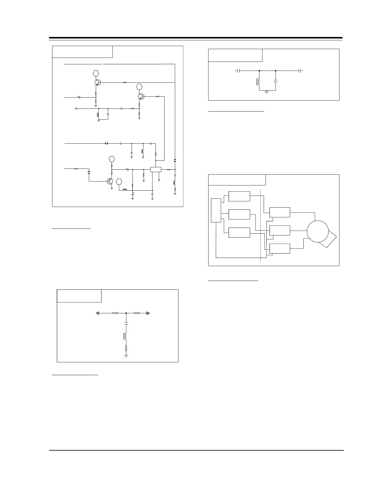
BAND PASS FILTER
To obtain the chroma information from a composite
video signal a BPF is used. The theory says that the
filter is centered at 3.58 MHz with 1MHz bandwidth.
Each component on a filter can affect the appearance
of the image. The next circuit shown is the band pass
circuit.
C2408M
1000pF
50V
L2402
6.8uH
C2409M
62pF
50V
C2410M
220pF
50V
From Comb filter
To AV Switch
BAND PASS FILTER
VIDEO OUTPUT BOARD
The signal is first uncoupled at the output of the video
processor. Three transistors in the emitter follower
configuration do this. Then the signal is amplified to
the levels required for a good image on the CRT by the
Video output board. On each amplifier there is a
dedicated section for sensing the cathode current for
the AKB system.
GREEN VO
AMPLIFIER
RED VO
AMPLIFIER
BLUE VO
AMPLIFIER
GREEN
PREDRIVER
RED
PREDRIVER
BLUE
PREDRIVER
VIDEO
PROCESSOR
CRT
VIDEO OUPUT BOARD
AKB SENSE
CRT/VIDEO MODULE
The Video Output Amplifier circuitry is divided into 4
sections. One section is the support circuitry for the
CRT (G2 circuit, for example). The other sections are
RGB amplifiers (one for each color signal). The locations
for all the components are numbered according to these
four sections. x510x references components in CRT
support circuitry, x520x components are the Red
section, x514x components are the Green section, and
x516x components are the Blue section. So, for example,
resistor R5125 in the Red section has the same function
as R5145 in the Green section and R5165 in the blue
section. For the purpose of analysis, the explanation
below is based on the Red section.
The principal part of the Red amplifier is IC5121. This
IC is an operational amplifier, configured as an inverting
amplifier. The inverting input is on pin 2 and the non-
inverting input is on pin 4. The Feedback resistor is
R5125. It has a gain peaking network between pin 1
and pin 3. This network is internally connected to the
collectors of the differential input transistors.