SR23 - 923-03509 3-4 CS - SERVICING
CIRCUIT OVERVIEW (continued)
The input signal is connected to the inverting input of
the amplifier through resistor R5121 to avoid Hi
frequency oscillations. The non-inverting input is
connected to a voltage bias formed by resistors R5101
and R5102.
+12
VDC
R5101
6.8K
R5102
2.4K
VB
C5122
47uF
50V
C5121M
15pF
50V
C5124
0.047pF
50V
C5123M
0.01uF
50V
R5122M
1K
R5123M
820
C5132M
0.01uF
50V
R5125
27K
3W
R5169
47
1 RC-
2 VIN
3 RC+
4 VB
5 IN
6 12V
7 IK
8 GND
9 NC
10 200V
11 NC
12 OUT0
13 OUT
C5125
0.22MFD
250V
+220
VDC
R5126
47K
1/2W
TDA6120Q
IC5121
F-53938
221-01404 126-03390-08
R5128
470
1/2W
C5126
560pF
500V
Q5121
121-01356A
B
E
C
L5121
0
D5108
103-00415-02A
+220
VDC
Video Output Amp (Red)
The C5122 is for AC decoupling and C5123 is for Hi
Frequency filter purposes (one for each IC). The IC takes
this voltage bias as a reference voltage for the input
signal. Therefore, by means of moving this reference
voltage, the black level is established. The reference
voltage is the same for the three-color amplifiers.
The cathode output is from pin 12 of the IC. This signal
is passed through transistor Q5121 with the purpose
of sampling the cathode current. This cathode output
also uses resistors R5127, R5128, and the coil L5121
for peaking improvement.
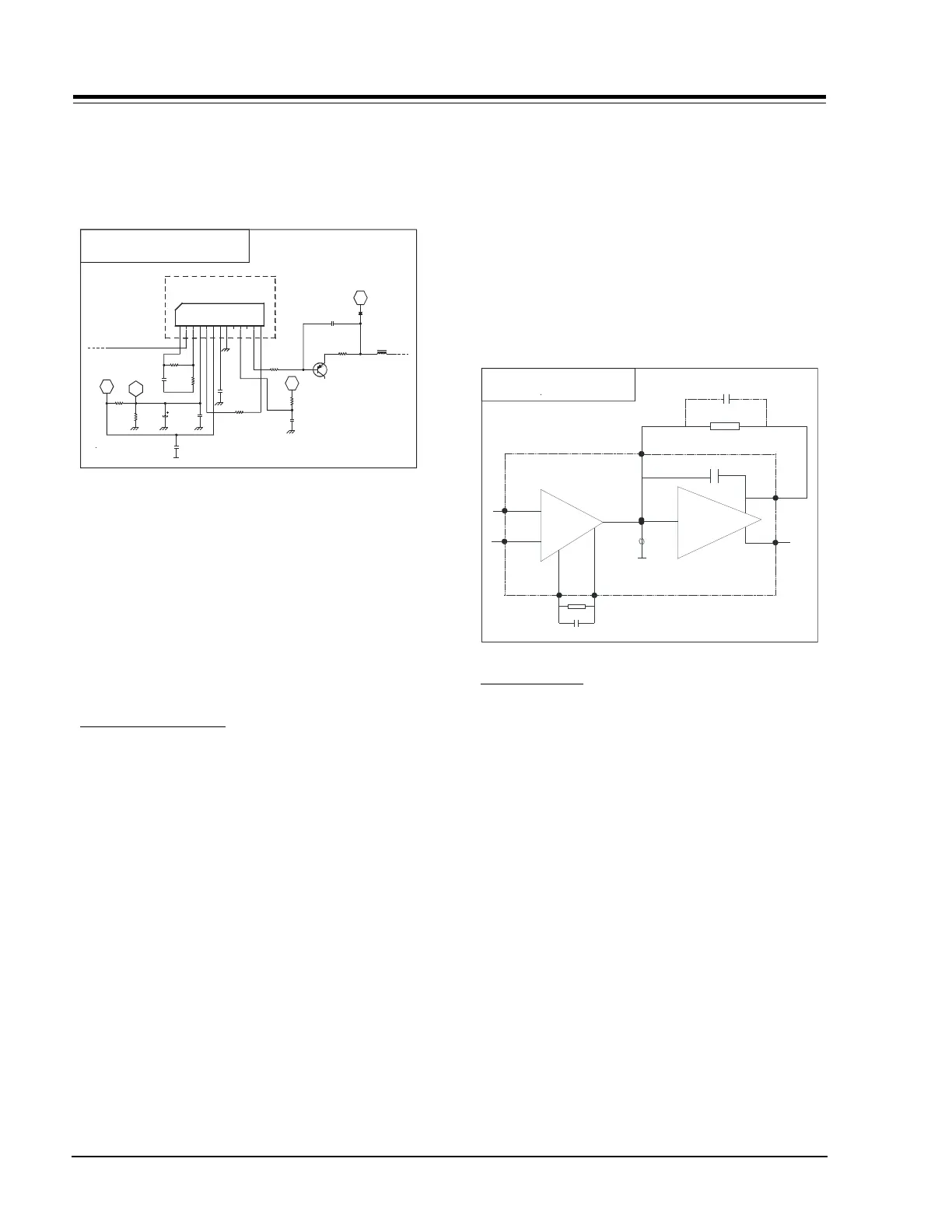
VIDEO OUTPUT AMP IC
IC5121 consists of one monolithic video output
amplifier. It is called a transadmittance-transimpedance
amplifier because it can be split into two amplifier
stages in series. The first stage is a voltage to current
stage (transadmittance) and the second stage is a
current to voltage stage (transimpedance).
At the second stage voltage to current feedback is
applied by resistor (R5125) connected from out (pin
13) to in (pin 5). The transadmittance of the first stage
can be chosen by means of a resistor between pin 1
and pin 3, represented on this circuit by R5122.
The signal input is through a differential pair of
transistors. The signal is connected on pin 2 (Vin). The
input configuration consists of a bipolar NPN transistor
in a long tailed pair configuration. Input current is
30µA type.
Black current data pin (7) is not used. Instead of this
pin, the current is sensed externally by means of
transistor Q5121.
Video output current is delivered by a quasi-
complementary class A/B push-pull stage designed in
DMOS technology which can source and sink a current
of 100mA for video output voltages of 125Vp-p. A
feature of this output stage is the low saturation voltage
(typ. 4V) and the low voltage drop at high level (typ.
Vdd-6V).
Frequency response is improved by means of a capacitor
(C5121) in series with a resistor (R5123) connected
between pins 1 and 3 of the IC. The values of these
elements are a compromise between bandwidth,
overshoot, and ringing.
13
12
I/U
OUT
OUT
CI int
IDC
4.5mA
5
Vin -
Vin +
Rf
CI ext
2
4
TDA6120Q
U/I
RC-
RC+
1
3
Ci
Ri
Video Output Amp IC
AKB OPERATION
The auto cut off system is intended for stabilization of
the black current and to compensate for CRT aging.
The video processor adds 3 pulses on the last portion
of the vertical blanking interval (one for each color).
The currents on the cathode for each pulse are sensed
and sent back to the video processor for correction.
Each pulse is actually a complete horizontal line with a
video level of approximately 8 Ire’s. These pulses are
slightly closing the vertical scan. They appear as a set
of 3 lines on the top of the image.
The Cathode current is sensed by a PNP transistor
(Q51X1). The three sensed currents are tied together
and send back to the video processor. On the main
board this current signal is converted to voltage and
sent to the video processor (pin 41 of ICX2200).
The video processor internally resolves the current level
of each color, compares it to its internal reference, and
makes an adjustment.