8
…4 ELECTRICAL INSTALLATION
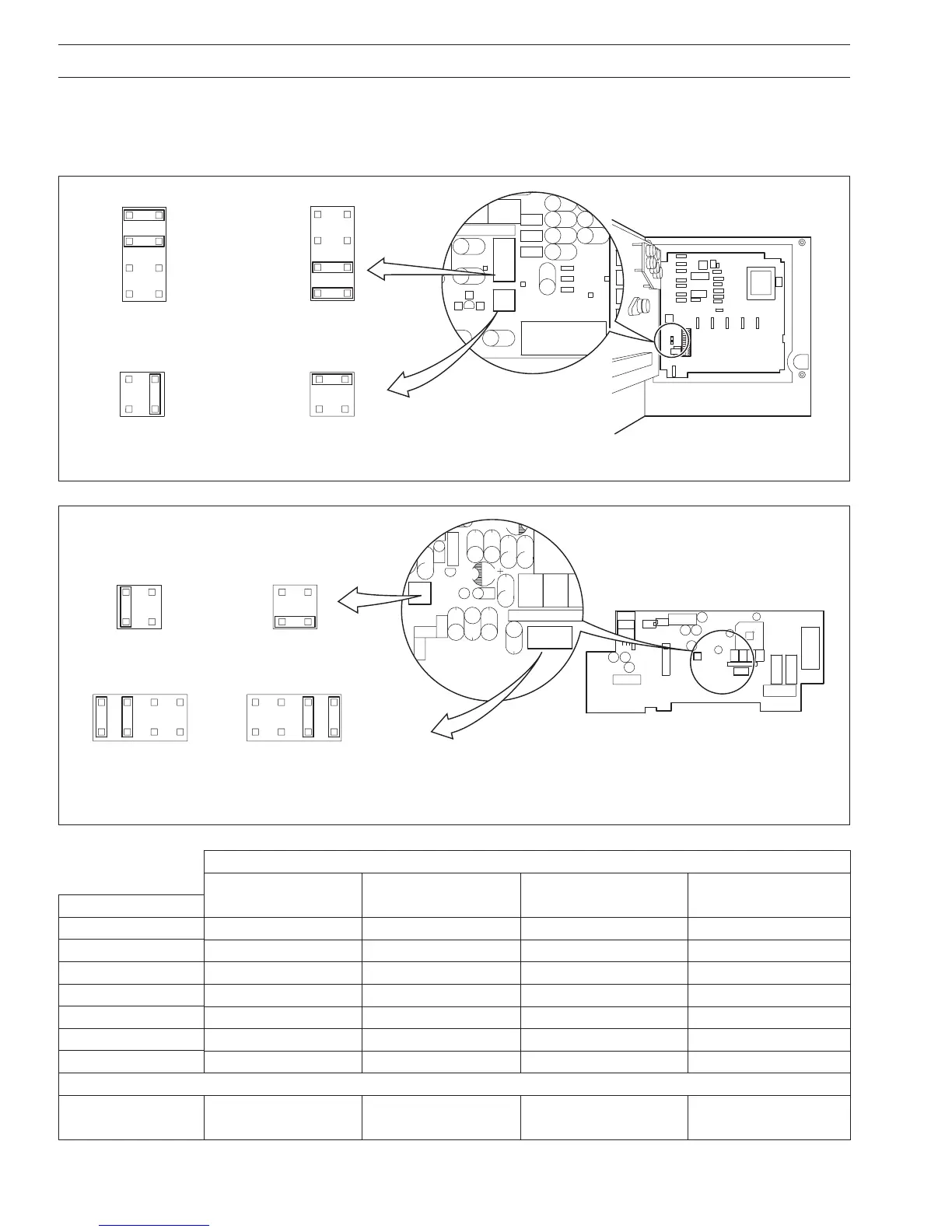
Position 1
Position 2
Position 3
Position 4
Position 5
Position 6
IC5
PL1
8
5
4
1
PL8
4
1
IC12
C87
C86
C85
C18
TR10
R17
R18
R16
R20
R25
R50
R22
R15
R48
R49
R40
mV THC mA V RTD & Resistance
PL1
PL1
2-wire Transmitter All Other Input Types
PL8PL8
2
1
3
4
1
4
8
5
2
1
3
4
1
4
8
5
Fig. 4.3 Selecting the Input Type (Main Board)
Fig. 4.4 Selecting the Input Type (I/O Modules)
Table 4.1 Thermocouple Compensating Cable
PL3 PL3
2
1
3
4
2
1
3
4
All Other Input Types
2-wire Transmitter
PL1 PL1
5
8
4
1
5
8
4
1
mA V RTD & ResistancemV THC
R20
R46
R45
R21
R23
R30
R29
R25
R22
R47
D6
D24
C25
C18C19
C6
C36
C37
0VI
IC8
14
PL3
4
5
PL1
elbaCgnitasnepmoC
3481SB1.69CMISNA41734NID03.oNtraP7394SB
elpuocomrehTfoepyT+–esaC+– esaC+–esaC+– esaC
)K(lA-iN/rC-iNnworBeulBdeRwolleYdeRwolleYdeRneerGneerGneerGetihW*neerG
)E(iN-uC/rC-iN———teloiVetihW*teloiV
)N(lisiN/lisirciNegnarOeulBegnarOegnarOdeRegnarO—kniPetihWkniP
)SdnaR(hR-tP/tPetihWeulBneerGkcalBdeRneerGdeRetihWetihWegnarOetihW*egnarO
)B(hR-tP/hR-tP———yerGetihW*yerG
)T(iN-uC/uCetihWeulBeulBeulBdeReulBdeRnworBnworBnworBetihW*nworB
)J(noC/eFwolleYeulBkcalBetihWdeRkcalBdeReulBeulBkcalBetihW*kcalB
stiucricefasyllacisnirtnirofeulBesaC*
)01734NID(noC/eF——
01734NID
—
deR/eulBeulBeulB
4.2.1 Selecting the Analog Input Type(s) – Figs. 4.3 and 4.4
Plug-in links are used to select the input type:
Channel 1 PL1 & PL8 on the main p.c.b. (Fig. 4.3)
Channels 2 to 4 PL1 & PL3 on the module (Fig. 4.4)
 Loading...