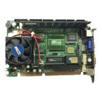
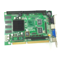
AR-B1579 User's Guide
3-5
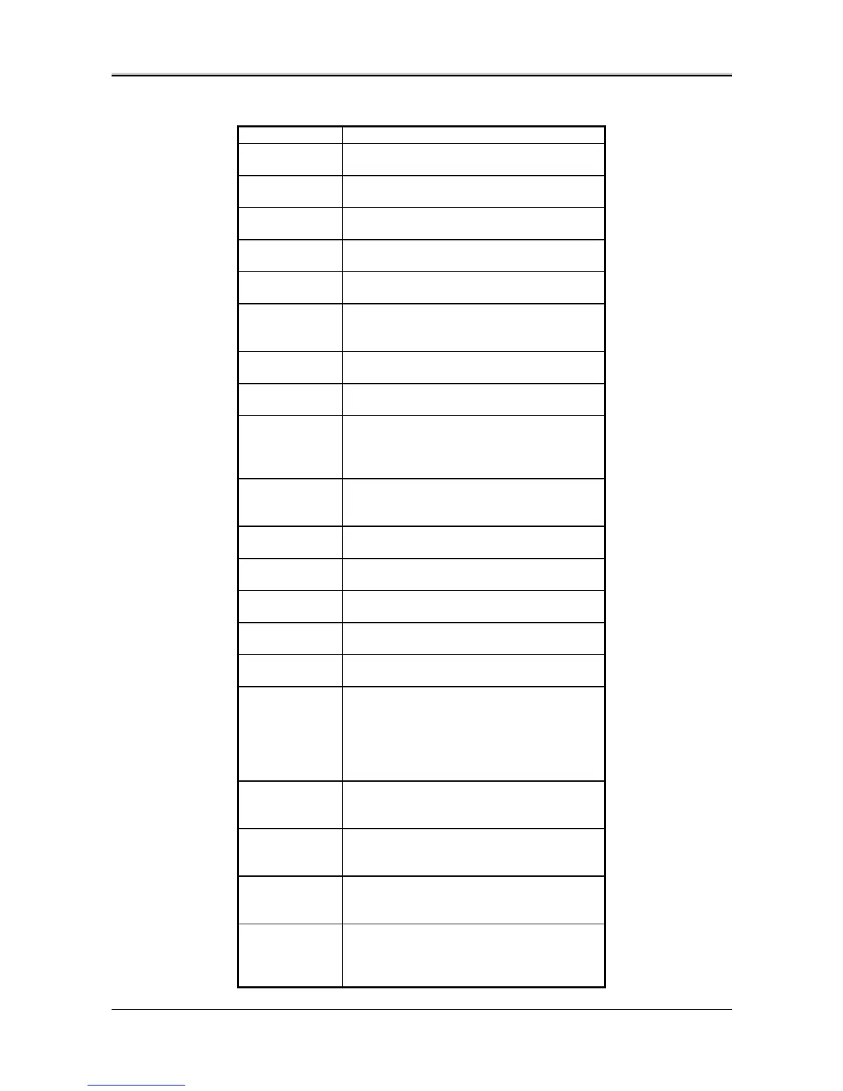
(3) I/O Channel Signal Description
Name Description
BUSCLK [Output]
The BUSCLK signal of the I/O channel is asynchronous
to the CPU clock.
RSTDRV [Output]
This signal goes high during power-up, low line-voltage
or hardware reset
SA0 - SA19
[Input / Output]
The System Address lines run from bit 0 to 19. They are
latched onto the falling edge of "BALE"
LA17 - LA23
[Input/Output]
The Unlatched Address line run from bit 17 to 23
SD0 - SD15
[Input/Output]
System Data bit 0 to 15
BALE [Output]
The Buffered Address Latch Enable is used to latch SA0
- SA19 onto the falling edge. This signal is forced high
during DMA cycles
-IOCHCK [Input]
The I/O Channel Check is an active low signal which
indicates that a parity error exist on the I/O board
IOCHRDY
[Input, Open collector]
This signal lengthens the I/O, or memory read/write
cycle, and should be held low with a valid address
IRQ 3-7, 9-12, 14, 15
[Input]
The Interrupt Request signal indicates I/O service
request attention. They are prioritized in the following
sequence : (Highest) IRQ 9, 10, 11, 12, 13, 15, 3, 4, 5,
6, 7 (Lowest)
-IOR
[Input/Output]
The I/O Read signal is an active low signal which
instructs the I/O device to drive its data onto the data
bus
-IOW [Input/Output]
The I/O write signal is an active low signal which
instructs the I/O device to read data from the data bus
-SMEMR [Output]
The System Memory Read is low while any of the low 1
mega bytes of memory are being used
-MEMR
[Input/Output]
The Memory Read signal is low while any memory
location is being read
-SMEMW [Output]
The System Memory Write is low while any of the low 1
mega bytes of memory is being written
-MEMW
[Input/Output]
The Memory Write signal is low while any memory
location is being written
DRQ 0-3, 5-7 [Input]
DMA Request channels 0 to 3 are for 8-bit data
transfers. DMA Request channels 5 to 7 are for 16-bit
data transfers. DMA request should be held high until
the corresponding DMA has been completed. DMA
request priority is in the following sequence:(Highest)
DRQ 0, 1, 2, 3, 5, 6, 7 (Lowest)
-DACK 0-3, 5-7
[Output]
The DMA Acknowledges 0 to 3, 5 to 7 are the
corresponding acknowledge signals for DRQ 0 to 3 and
5 to 7
AEN [output]
The DMA Address Enable is high when the DMA
controller is driving the address bus. It is low when the
CPU is driving the address bus
-REFRESH
[Input/Output]
This signal is used to indicate a memory refresh cycle
and can be driven by the microprocessor on the I/O
channel
TC [Output]
Terminal Count provides a pulse when the terminal
count for any DMA channel is reached