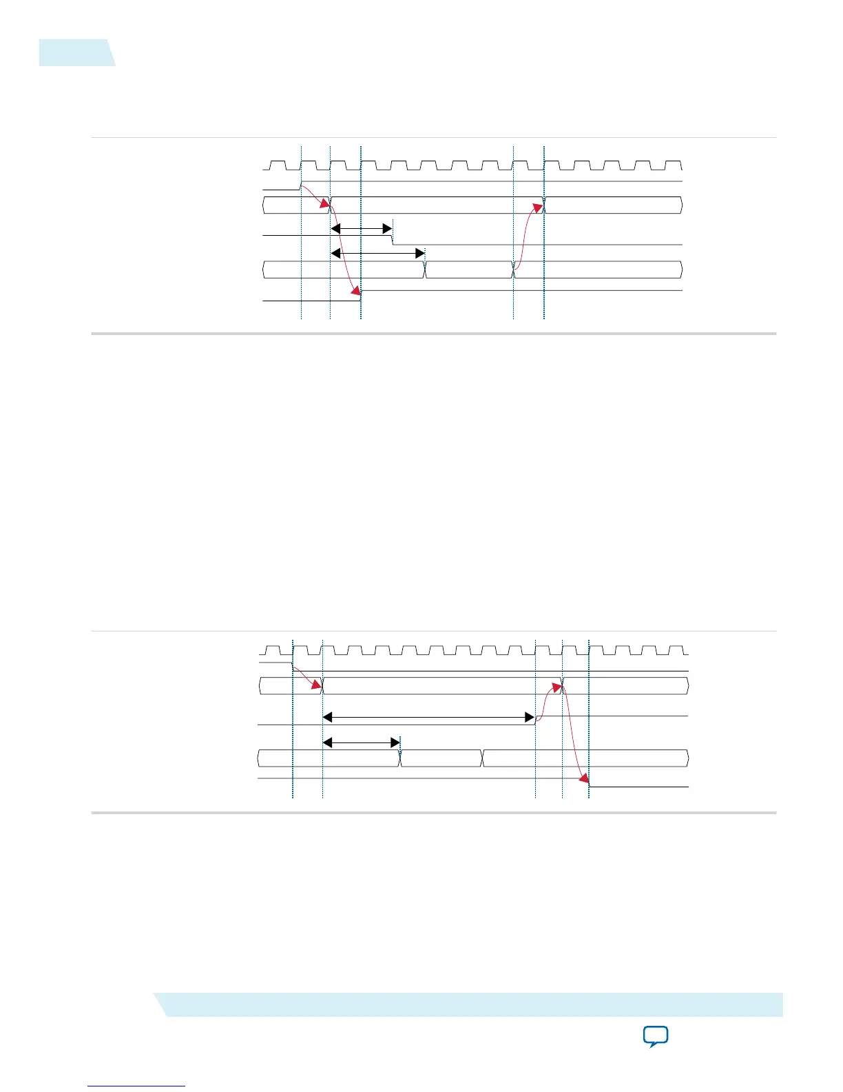
Entering Sleep Mode
Figure 3-3: Entering Sleep Mode Timing Diagram
clk
sleep
current_state
ioe
clk_ena[15:0]
sleep_status
Awake Entering Sleep
16’hFFFF Disabling
16’h0000
T1
T2
The following sequence occurs when the device enters sleep mode:
1. An internal or external request drives the sleep signal high, forcing the device to go into sleep mode.
2. After a delay of T1, the power management controller powers down all the I/O buffers by de-asserting
ioe signal that connects to oe and nsleep ports of the I/O buffers.
3. After a delay of T2, the power management controller turns off all GCLK networks by disabling
clk_ena[15:0] signal from LSB to MSB. After three clock cycles, the clk_ena[15:0] signal is fully
disabled and transits into the sleep state.
4. The power management controller remains in sleep state until the sleep signal is de-asserted.
5. User logic will latch the running counter value before entering the sleep state and output to
cnt_sleep_enter port. The running counter is then frozen.
6. gpio_pad_output (GPIO) is tri-stated when ioe is de-asserted.
Exiting Sleep Mode
Figure 3-4: Exiting Sleep Mode Timing Diagram
clk
sleep
current_state
ioe
clk_ena[15:0]
sleep_status
Sleep Exiting Awake
16’hFFFFEnabling
16’h0000
T4
T3
3-4
Entering Sleep Mode
UG-M10PWR
2015.11.02
Altera Corporation
Power Management Controller Reference Design
Send Feedback
 Loading...


