The following sequence occurs when the device exits sleep mode:
1. An internal or external request drives the sleep signal low, forcing the device to exit sleep mode.
2. After a delay of T3, the power management controller turns on all GCLK networks by enabling
clk_ena[15:0] signal from LSB to MSB. After three clock cycles, the clk_ena[15:0] signal is fully
enabled and all GCLK networks are turned on.
3. After a delay of T4, the power management controller powers up all the I/O buffers by asserting the
ioe signal.
4. The power management controller remains in awake state until the sleep signal is asserted.
5. User logic will latch the running counter value before the awake state and output to cnt_sleep_exit
port. The running counter is then release from freeze.
6. gpio_pad_output (GPIO) is driving its output value when ioe is asserted.
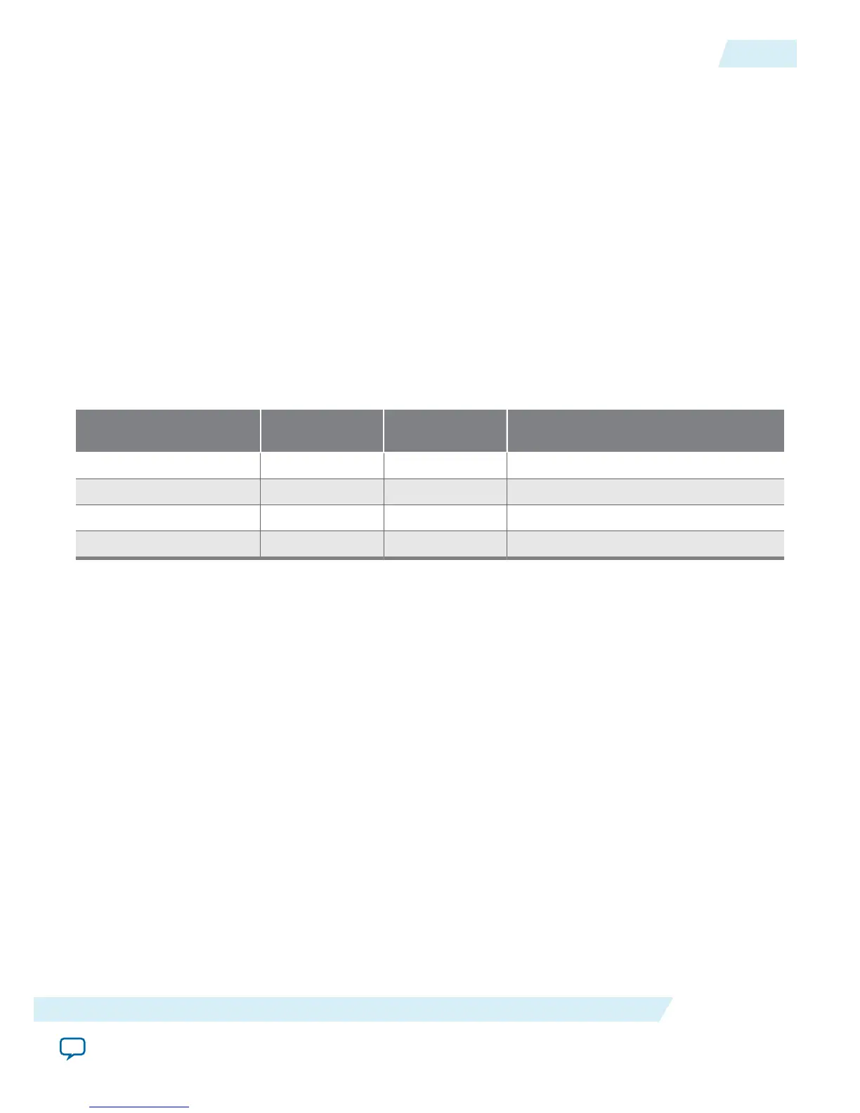
Timing Parameters
The following table lists the definition and minimum value of the T1, T2, T3, and T4 parameters in the
entering sleep mode timing diagram and exiting sleep mode timing diagram, respectively.
Table 3-2: T1, T2, T3, and T4 Parameters Minimum Value and Definition
Parameter Width (bits) Minimum Value
(Decimal)
Description
T1 6 1 ioe disable timing.
T2 6 11 clk_ena disable timing.
T3 6 1 clk_ena enable timing.
T4 6 40 ioe enable timing.
T1, T2, T3, and T4 can be increased based on your system requirement.
Hardware Implementation and Current Measurement
This design is implemented using the 10M50DAF484C8 device. You can implement this design using any
MAX 10 device. This design runs on the MAX 10 Development Kit Board to show current and power
relative between user mode and sleep mode.
The resource utilization of this design is as follows:
• 42,000 LEs (84% of total LEs)—gray counter top module utilizes most of the LEs in the device
• 33 I/O pins (9% of total pins)—covering 3 input pins and 30 output pins
The current in this design is measured using a current monitor component (the Linear Technologies LTC
2990). The measured current is further processed by a pre-programmed design in a MAX II device. The
UG-M10PWR
2015.11.02
Timing Parameters
3-5
Power Management Controller Reference Design
Altera Corporation
Send Feedback

 Loading...


