2–4 Chapter 2: Board Components
Featured Device: MAX V CPLD
MAX V CPLD Development Board Reference Manual September 2015 Altera Corporation
Table 2–3 lists the MAX V CPLD device component reference and manufacturing
information.
I/O Resources
The 5M570ZF256C5N device support two I/O banks and each of these banks support
all the LVTTL, LVCMOS, LVDS, and RSDS standards.
Figure 2–2 illustrates the bank organization for the 5M570ZF256C5N device in a
256-pin FBGA package.
Table 2–4 lists the MAX V CPLD device pin count and usage by function on the
development board.
Table 2–3. MAX V CPLD Device Component Reference and Manufacturing Information
Board Reference Description Manufacturer
Manufacturing
Part Number
Manufacturer
Website
U5
MAX V CPLD, 256-pin FBGA
package, 570 LEs, lead-free.
Altera
Corporation 5M570ZF256C5N www.altera.com
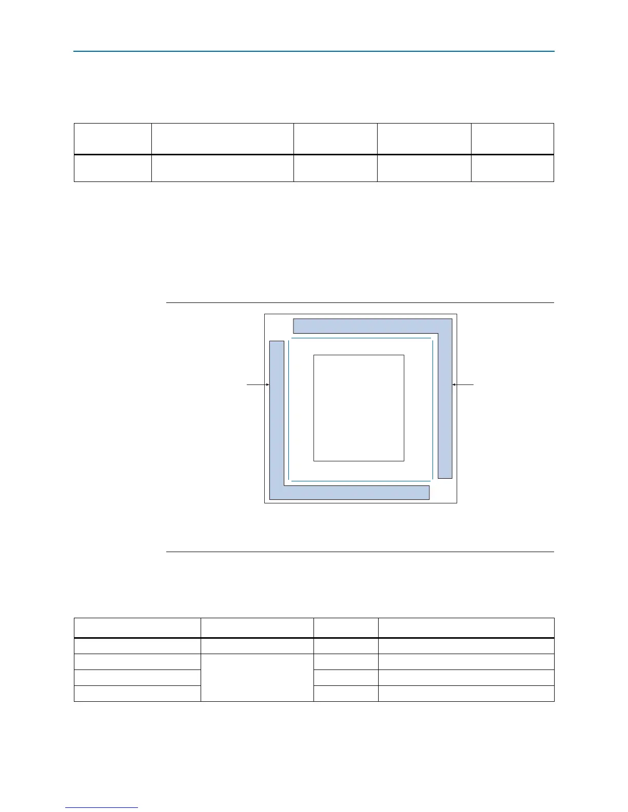
Figure 2–2. 5M570ZF256C5N Device I/O Bank Diagram (Note 1)
Note to Figure 2–2:
(1) This figure is a top view of the silicon die and is a graphical representation only. Refer to the pin list and the Quartus II
software for exact pin locations.
I/O Bank 1
I/O Bank 2
5M570ZF256C5N
Table 2–4. MAX V CPLD Device I/O Pin Count and Usage (Part 1 of 2)
Function I/O Standard I/O Count Special Pins
40-pin GPIO Header A 3.3-V CMOS 36 —
40-pin GPIO Header B
1.2-V to 3.3-V
36 —
PC Speaker Header 8 —
DC Motor Headers 18 —