September 2015 Altera Corporation MAX V CPLD Development Board Reference Manual
1. Overview
Introduction
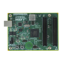
This document describes the hardware features of the MAX
®
V CPLD development
board, including the detailed pin-out and component reference information required
to create custom CPLD designs that interface with all components of the board.
General Description
The MAX V CPLD development board provides a hardware platform for developing
and prototyping low-cost, low-power CPLD designs, as well as to demonstrate the
features of the MAX V CPLD device.
To facilitate the development of MAX V CPLD designs, the board provides connectors
to interface to external functions or devices.
f For more information on the MAX V CPLD device family, refer to the MAX V Device
Handbook.
Board Component Blocks
The board features the following major component blocks:
■ MAX V CPLD 5M570ZF256C5N in a 256-pin FineLine BGA (FBGA) package
■ 570 logic elements (LEs)
■ 440 equivalent macrocells
■ 8,192-bits user flash memory (UFM)
■ 4 global clocks
■ 159 user I/Os
■ 1.8-V core power
■ MAX II EPM240M100C4N CPLD in the 100-pin Micro FBGA (MBGA) package
■ On-Board configuration circuitry
■ Embedded USB-Blaster
TM
for use with the Quartus
®
II Programmer
■ On-Board connectors
■ Type-B USB connector (as power source and communication port)
■ Two general purpose I/O (GPIO) 2×20-pin 0.1-inch expansion headers
■ One 4-pin PC speaker header
■ Two 2×3-pin DC motor headers
■ On-Board clocking circuitry
■ 10-MHz single-ended external oscillator

 Loading...