Chapter 2: Board Components 2–3
Featured Device: MAX V CPLD
September 2015 Altera Corporation MAX V CPLD Development Board Reference Manual
Featured Device: MAX V CPLD
The MAX V CPLD development board features the MAX V CPLD 5M570ZF256C5N
device (U5) in a 256-pin FBGA package.
Table 2–2 describes the features of the MAX V CPLD 5M570ZF256C5N device.
f For more information about MAX V CPLD device family, refer to the MAX V Device
Handbook.
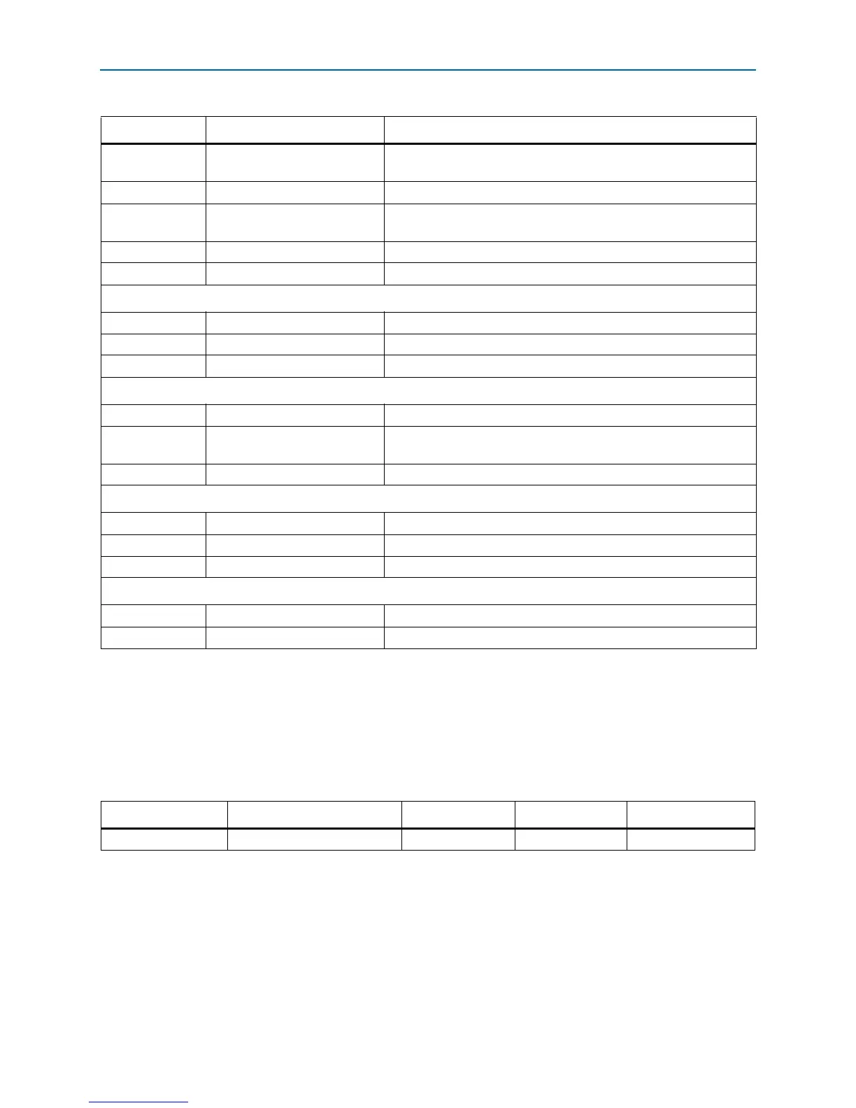
U3 USB 2.0 PHY
A FTDI USB 2.0 PHY device to configure the CPLD over embedded
USB-Blaster.
U4 CPLD MAX II CPLD EPM240M100.
J13, J14 JTAG header
Footprint (at the bottom of the board) to mount a JTAG header. The
header allows direct-access to devices in the JTAG connection.
D1 Power LED Illuminates when 5-V USB power is present.
D3 USB LED Illuminates to indicate USB-JTAG activity.
Clock Circuitry
J1 10-MHz oscillator 10-MHz single-ended input clock for the MAX V CPLD.
X1 6-MHz oscillator 6-MHz input clock for the FTDI USB 2.0 PHY device.
Y1 24-MHz oscillator 24-MHz input clock for the MAX II CPLD EPM240M100.
Connectors
J6, J7 GPIO headers Two general-purpose 2x40-pin 0.1-inch expansion headers.
J9 PC speaker header
A 4-pin PC speaker header which connects to the MAX V CPLD I/O
bank 2.
J5, J10 DC motor headers Two motor headers which connects to the MAX V CPLD I/O bank 2.
General User Input/Output
D7, D8 User LEDs Two user LEDs. Illuminates when driven low.
S1, S2 User push-button switches Two user push-button switches. Driven low when pressed.
CPB1 Capacitor sense button One capacitive touch-sense user-defined button.
Off-Chip EEPROM
U6 I
2
C EEPROM Footprint to install an I
2
C serial EEPROM
U8 SPI EEPROM Footprint to install a SPI EEPROM.
Table 2–1. MAX V CPLD Development Board Components (Part 2 of 2)
Board Reference Type Description
Table 2–2. MAX V CPLD 5M570ZF256C5N Device Features
Equivalent LEs User Flash Memory (bits) User I/Os Global Clocks Package Type
570 8192 159 4 256-pin FBGA