1–2 Chapter 1: Overview
Development Board Block Diagram
MAX V CPLD Development Board Reference Manual September 2015 Altera Corporation
■ General user I/O
■ LEDs and display
■ Two CPLD user LEDs
■ One USB status LED
■ One power status LED
■ Push-Button switches
■ Two user-defined push-button switches
■ One capacitor sense push-button switch
■ Mechanical
■ 4.1” × 3.1” board
Development Board Block Diagram
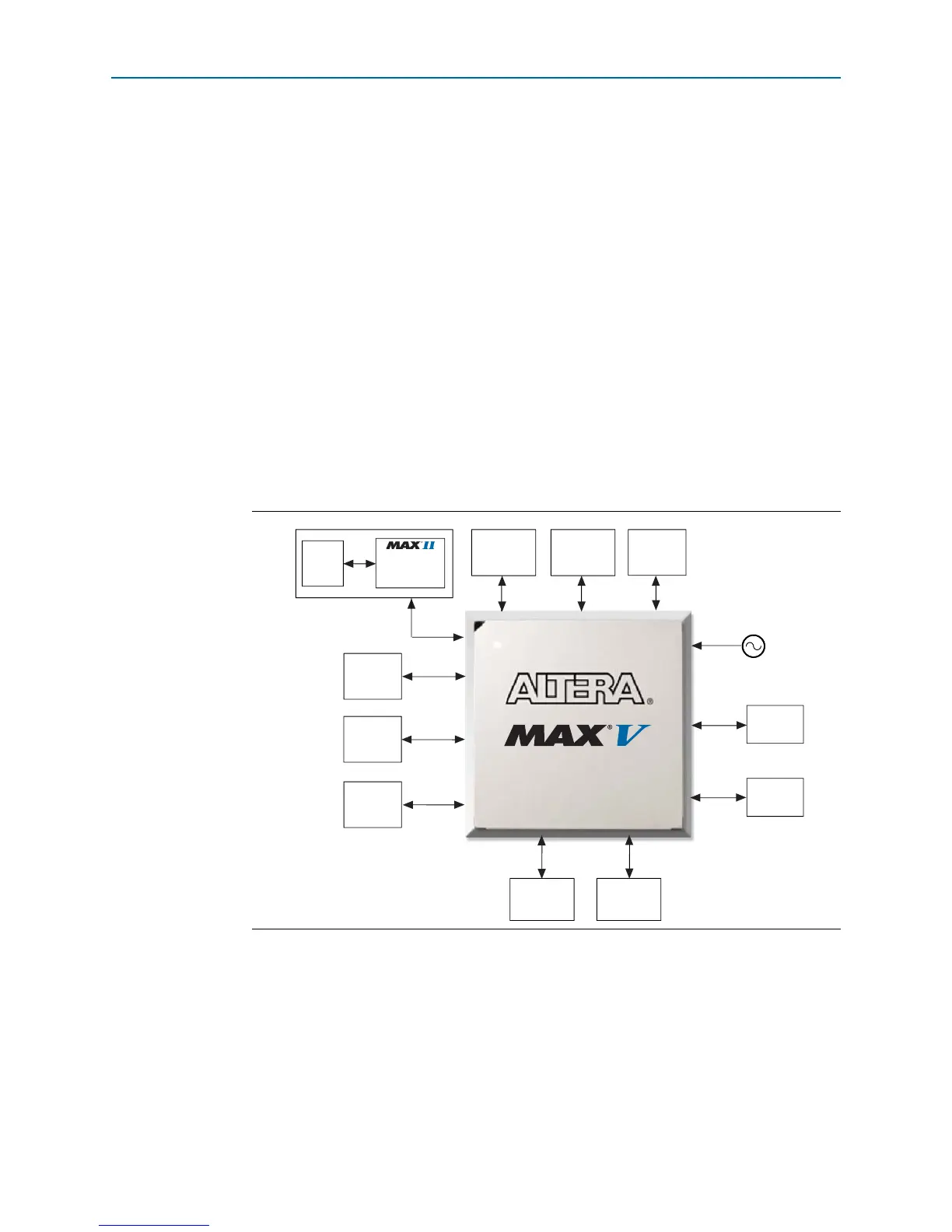
Figure 1–1 shows the block diagram of the MAX V CPLD development board.
Handling the Board
When handling the board, it is important to observe the following static discharge
precaution:
c Without proper anti-static handling, the board can be damaged. Therefore, use
anti-static handling precautions when touching the board.
Figure 1–1. MAX V CPLD Development Board Block Diagram
DC Motor
Header 1
EPM240M100
Embedded
USB-Blaster
USB
2.0
x1
x9
x2
JTAG Chain
GPIO
Header 2
EP5M570ZF256N
SPI x4
User LEDs
Push-Button
Switches
x2
x36
I
2
C x2
10 MHz Oscillator
GPIO
Header 1
x36
PC Speaker
Header
Capacitor
Sense
Push-Button
Switch
x8
x9
DC Motor
Header 2
EEPROM
EEPROM