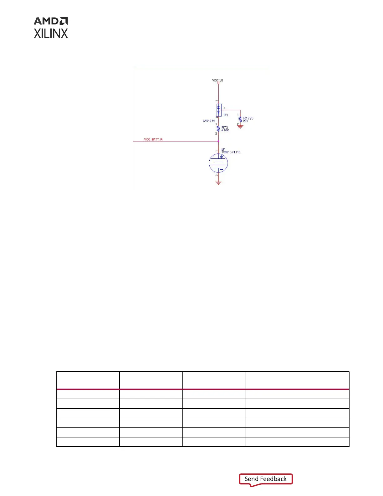
Figure 5: Encryption Key Backup Circuit
X26015-080522
The Seiko TS621E rechargeable 1.5V lithium buon-type baery B1 is soldered to the board
with the posive output connected to the XCVP1802 ACAP U1 VCC_BATT bank pin AN20. The
baery supply current IBATT specicaon is 150 nA maximum when board power is o. Baery
B1 is charged from the VCC1V8 1.8V rail through a 2 series diode with the rst forward drop to
yield between 0.24V to 0.46V over temperature per xed 5 mA load, R1725, and liming 1.56V
max at the ACAP pin, PSVBATT. The second diode and 4.7 kΩ current limit resistor allows the
baery to trickle charge and prevent baery B1 from back powering R1725.
I/O Voltage Rails
The XCVP1802 ACAP PL I/O bank voltages on the VPK180 board are listed in the following
table. See LPD MIO[23]: VADJ_FMC Power Rail for more details on the VADJ_FMC power rail.
Note: The VPK180 evaluaon board is shipped with VCC_PMC set to 0.88V, allowing for overdrive. See
the Versal Premium Series Data Sheet: DC and AC Switching Characteriscs (DS959) for more informaon. See
the Versal ACAP Technical Reference Manual (AM011) for more informaon about Versal ACAP
conguraon opons.
Table 6: I/O Voltage Rails
ACAP (U1) Bank
Power Supply Rail
Net Name
Voltage Description
XPIO Bank 700 VCC1V1_LP4 1.1V LPDDR4 TRIP1 CH1
XPIO Bank 701 VCC1V1_LP4 1.1V LPDDR4 TRIP1 CH0, LPDDR4 TRIP1 CH1
XPIO Bank 702 VCC1V1_LP4 1.1V LPDDR4 TRIP1 CH0
XPIO Bank 703 VCC1V1_LP4 1.1V LPDDR4 TRIP2 CH1
XPIO Bank 704 VCC1V1_LP4 1.1V LPDDR4 TRIP2 CH0, LPDDR4 TRIP2 CH1
XPIO Bank 705 VCC1V1_LP4 1.1V LPDDR4 TRIP2 CH0
Chapter 3: Board Component Descriptions
UG1582 (v1.0) February 21, 2023 www.xilinx.com
VPK180 Board User Guide 24