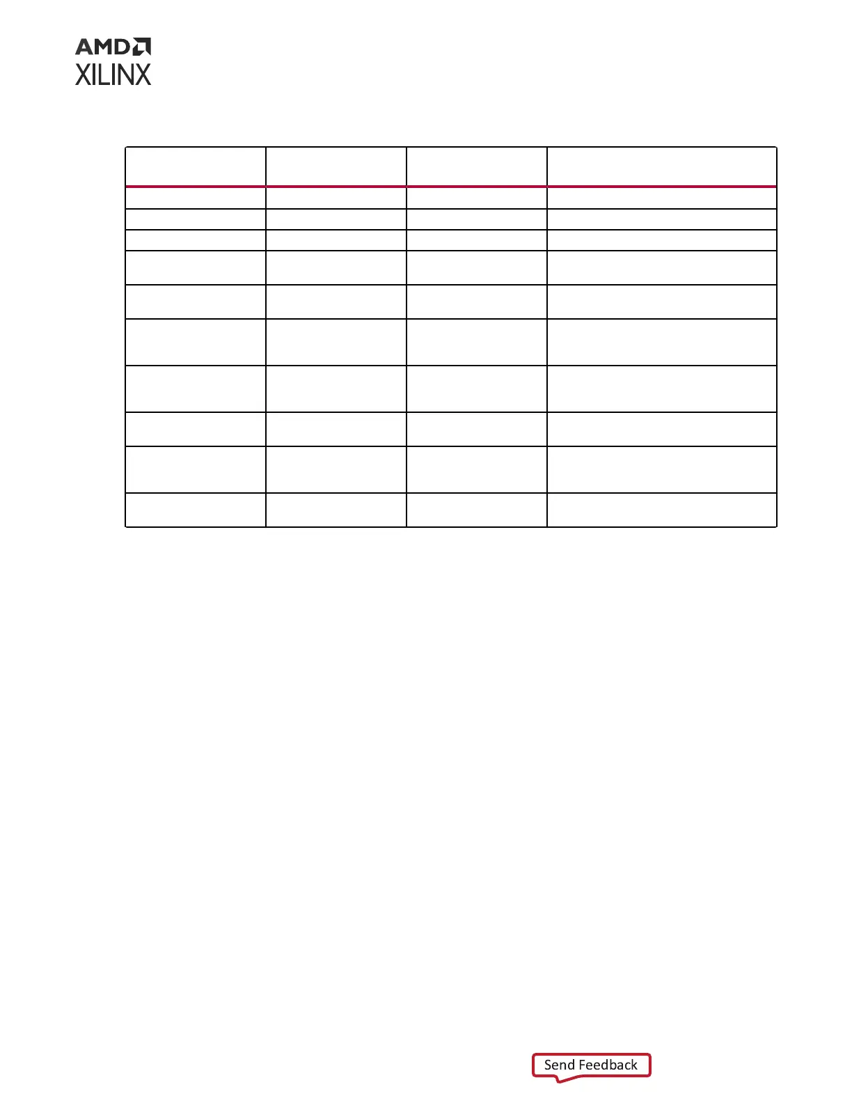
Table 6: I/O Voltage Rails (cont'd)
ACAP (U1) Bank
Power Supply Rail
Net Name
Voltage Description
XPIO Bank 706 VCC1V1_LP4 1.1V LPDDR4 TRIP3 CH1
XPIO Bank 707 VCC1V1_LP4 1.1V LPDDR4 TRIP3 CH0, LPDDR4 TRIP3 CH1
XPIO Bank 708 VCC1V1_LP4 1.1V LPDDR4 TRIP3 CH0
XPIO Bank 709 VADJ_FMC
1
1.5V (default) FMCP1_LA[17:18]_CC, FMCP1_LA[19:33],
FMCP1_SYNC, FMCP_CLK1, SFPDD[1:2] I/O
XPIO Bank 710 VADJ_FMC
1
1.5V (default) FMCP1_LA[00:01]_CC, FMCP1_LA[02:16],
FMCP1_CLK0, SFPDD[3:4] I/O
XPIO Bank 711 VCC1V5 1.5V 8A34001_GPIO_[14:15],
SYSCTLR_GPIO[0:15], QSFPDD[1:6] I/O,
GPIO_PB[0:1]
XPIO Bank 712 VCC1V5 1.5V GPIO_DIP_SW[0:3], GPIO_LED_[0:3]_LS,
UART1, OSFP control signals, TRACE
signals, 8A34001_GPIO[0:7;10:13]
PMC MIO 500 VCCO_MIO 1.8V SYSMON, USB ULPI 2.0 interface, QSPI1/2
interface
PMC MIO 501 VCCO_MIO 1.8V SD bus power, I2C0/21, UART0, System
Controller I2C/trigger, SD card controls,
GEM reset
LPD MIO 502 VCCO_502 1.8V GEM interface/controls, power enables,
fan tach, fan PWM
Notes:
1. The VPK180 board is shipped with VADJ_FMC set to 1.5V by the ZU4 system controller.
LPDDR4 Component Memory
[Figure 3, callout 2, 3, 4]
The VPK180 XCVP1802 ACAP PL DDR memory interface performance is documented in the
Versal Premium Series Data Sheet: DC and AC Switching Characteriscs (DS959). The VPK180 board
LPDDR4 component memory interfaces adhere to the constraints guidelines documented in the
"PCB guidelines for Memory Interfaces" secon of the Versal ACAP PCB Design User Guide
(UG863). The VPK180 DDR4 component interface is a 40Ω impedance implementaon. Other
memory interface details are also available in the Versal ACAP Memory Resources Architecture
Manual (AM007). For more memory component details, see the Micron MT53D512M32D2DS
data sheet on the Micron website. For the most current part number, see the Bill of Materials
(BOM) located on the VPK180 Evaluaon Board website. The detailed ACAP connecons for the
feature described in this secon are documented in the VPK180 board XDC le, referenced in
Appendix B: Xilinx Design Constraints.
The VPK180 evaluaon board hosts three LPDDR4 memory systems, each with a component
conguraon of 2x (1x32-bit component).
Chapter 3: Board Component Descriptions
UG1582 (v1.0) February 21, 2023 www.xilinx.com
VPK180 Board User Guide 25