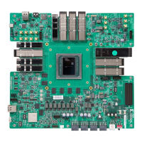
Figure 15: RGMII Ethernet
XCVP1802
ACAP
RGMII
LPD MIO[0:11 24:25]
GEM0 U198
DP83867
10/100/1000
PHY
MDIO
MII
J307
RJ45
25 MHz
Crystal
X27353-102722
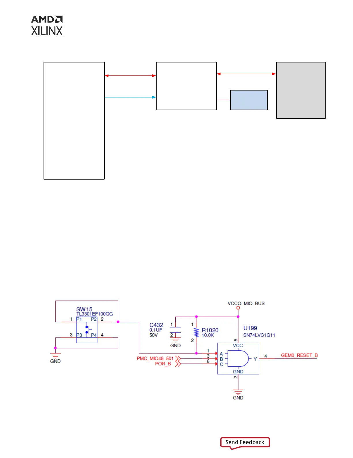
Ethernet PHY (Three Resets)
[Figure 3, callout 16]
The DP83867 PHY (GEM0 U198) is reset by its GEM0_RESET_B generated by dedicated
pushbuon switch (SW15) and PMC_MIO signals as shown in the following gure. The POR_B
signal generated by the TPS389001DSER U10 POR device is wired in parallel to each Ethernet
PHY reset circuit. The POR device is acvated by pushbuon SW2. See System Reset POR_B for
more details.
Figure 16: Ethernet PHY Reset Circuit
X26024-111821
Chapter 3: Board Component Descriptions
UG1582 (v1.0) February 21, 2023 www.xilinx.com
VPK180 Board User Guide 43