• I2C address 0x60
• LVDS dierenal output, total stability: 61.5 ppm
Programmable SI570 REF Clock
[Figure 3, callout 37]
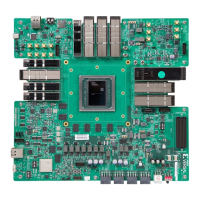
The VPK180 evaluaon board has an I2C programmable SI570 low-jier 1.8V CMOS single-
ended oscillator (U32). The 33.333 MHz REF_CLK clock signal is connected to XCVP1802 ACAP
U1 conguraon bank 503. At power-up, this clock defaults to an output frequency of
33.333333... MHz (33 + 1/3 MHz). User applicaons or the system controller can change the
output frequency within the range of 10 MHz to 945 MHz through the I2C bus interface. Power
cycling the VPK180 evaluaon board reverts this user clock to the default frequency of
33.333333... MHz (33 + 1/3 MHz).
• Programmable oscillator: Skyworks/Silicon Labs SI570JAC000900DG
• 10 MHz-945 MHz range, 33.333 MHz default
• I2C address 0x5D
• CMOS single-ended output, total stability: 61.5 ppm
Programmable MGT RC21008A REF Clocks
[Figure 3, callout 34]
The VPK180 evaluaon board has two I2C programmable RC21008A high-performance
frequency synthesizers (U298, U299) that provide excellent phase jier on reference clocks. The
output has been congured as a 1.8V LVDS output. The 156.25 MHz
RC21008A_GTCLK[1:2]_OUT[0:7] clock signals are connected to the XCVP1802 ACAP U1
transceiver banks. See the table in the Transceivers secon for connecvity. See schemac pages
61/62 for further details.
At power-up, this clock defaults to an output frequency of 156.25 MHz. User applicaons or the
system controller can change the output frequency within the range of 0.001 MHz to 650 MHz
through the I2C bus interface. Power cycling the VPK180 evaluaon board reverts this user clock
to the default frequency of 156.25 MHz.
• Programmable frequency synthesizer: Renesas RC21008A065#BB0
• 0.001 MHz-650 MHz range, 156.25 MHz default
• I2C address 0x09
• LVDS dierenal output
Chapter 3: Board Component Descriptions
UG1582 (v1.0) February 21, 2023 www.xilinx.com
VPK180 Board User Guide 48