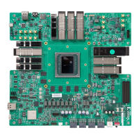
Block Diagram
A block diagram of the ZCU670 evaluaon board is shown in the following gure.
Figure 1: Evaluation Board Block Diagram
PS DDR4 SODIMM
64-bit
USB3.0
FMCP_HSPC_DP[4:6]
SFP[0:3]
FMCP_HSPC_DP[0:3]
SD3.0
PS_PMU_GPO[0:5]
PMU_INPUT
PS_GPIO1
SFP TX_DISABLE
USB3.0
ETHERNET RGMII
CONFIG.IF
JTAG IF
UART2
MSP430_UCA1
PL DDR4 Component
32-bit (4x8-bit)
SI538_PL_CLK
300MHz CLK
ADCIO x8
DACIO x8
8A34001 CLK in x1
Si5381 CLKO x1
Si5381 CLKinx1
ADCIO x8
DACIO x8
CLK104_SPI_MUX_SEL
TDD SMA x1
CPU_RESET
MPS430_GPIO
8A34001 CLKO x1
8A34001 CLKinx1
Si5381 CLKO x1
CLK104_PL_CLK
TDD SMA x1
PB/LEDs/CLK MUX SEL
SYSMON_I2C
PS PB/LED
UART0
PS_I2C0
PS_I2C1
QSPI_UPR
QSPI_LWR
PS_GPIO2
RFMC2.0 CON1
ADC_T1_CH0~CH3
ADC_T2_CH01/CH23
ADC_T0_CH0~CH3
RFMC2.0 CON2
DAC_T1_CH0~CH3
DAC_T0_CH0~CH3
X25678-111521
Board Features
The ZCU670 evaluaon board features are listed here. Detailed informaon for each feature is
provided in Chapter 3: Board Component Descripons.
• ZU67DR-2, FSVE1156 package
• Form factor: see Board Specicaons
• Conguraon from:
○ Dual QSPI
Chapter 1: Introduction
UG1532 (v1.0) March 30, 2022 www.xilinx.com
ZCU670 Board User Guide 5