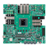
The ZCU670 provides a rapid prototyping plaorm that uses the XCZU67DR-2FSVE1156I
device. The ZU67DR contains many useful processor system (PS) hard block peripherals exposed
through the mul-use I/O (MIO) interface and a variety of FPGA programmable logic. The
following table lists a brief summary of the resources available within the ZU67DR.
Feature set overview, descripon, and ordering informaon is provided in the Zynq UltraScale+
RFSoC DFE Data Sheet: Overview (DS883).
Table 1: Zynq UltraScale+ RFSoC ZU67DR Features and Resources
Feature Resource Count
Digital front end Included
14-bit 2.95 GSPS RF-ADC with DDC 8
14-bit 5.9 GSPS ADC RF-DAC with DDC 2
14-bit 10 GSPS RF-DAC with DUC 8
APU: Quad-core Arm
®
Cortex
®
-A53 MPCore with CoreSight™ 1
RTPU: Dual-core Arm Cortex-R5F MPCore with CoreSight 1
HD I/O 96
HP I/O 312
MIO banks 3 banks, total of 78 pins
PS GTR 6 Gb/s transceivers 4 PS-GTRs
PL GTY 28 Gb/s transceivers 8 GTYs
System logic cells 489,300
CLB flip-flops 447,360
CLB LUTs 223,680
Maximum distributed RAM (Mb) 6.9
Block RAM blocks 648
UltraRAM blocks 160
DSP slices 1,872
100G Ethernet with RS-FEC 1
Board Specifications
Dimensions
Height: 12.225 inches (31.05 cm)
Width: 10.675 inches (27.11 cm)
Thickness: 0.122 inches (0.310 cm)
Note: A 3D model of this board is not available.
Chapter 1: Introduction
UG1532 (v1.0) March 30, 2022 www.xilinx.com
ZCU670 Board User Guide 8