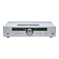
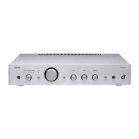
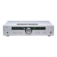
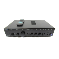
Amplifier & PSU Circuit Description
L882PB is the printed circuit board that provides the power supply
and output stage amplifiers for the A85 integrated and power
amplifiers.
Its function is to:
1. Drive the loudspeakers(!)
2. Provide an (always on) auxiliary 5VDC supply for the micro
controller and display interface
3. Receive logic signals from the micro controller to turn on
the main amplifier supply relay (mains) and connect either
pair of speaker output sockets
4. Send logic signals to the micro controller pertaining to the
state of the amplifiers (short circuit protection, DC offset
protection, thermal protection)
5. Receive and demodulate RC5 remote style control codes via
the rear panel jack and transmit them to the micro controller
6. Send a 12V trigger output via the rear panel jack for control
of an auxiliary power amp when the unit is on
7. Receive a 12V trigger input from the rear jack (for use in the
power amp only version)
8. Drive a pair of headphones via attenuating resistor networks
The power amplifier is a symmetrical, class B, bipolar junction
transistor output, current-feedback design (of which more later)
with DC-coupled signal and feedback paths, featuring an active
integrating voltage servo to control DC offsets.
It features ‘instantaneous’ safe operating area protection in
addition to sending a signal to the micro to turn off the output
relays in the event of user or thermal overload. Since it is a DC-
coupled design, the unit senses DC at the output and triggers the
micro to turn off the loudspeaker relays in the event of excessive
levels (possibly due to a faulty source component or short circuit
output transistor).
The output stage uses Sanken specialised ‘audio amplifier’ power
bipolar Darlington transistors which are optimised for use with this
type of topology. Consequently the unit has excellent measured
performance in terms of noise, slew rate, output impedance and
distortion (harmonic and intermodulated) and is essentially load
invariant (to a first order the measured performance is independent
of the load impedance).
L882 Circuit Sheet 1
The audio input to the amplifier is connected to SK102 (which
connects to the output of the preamp PCB). This signal is passed
on via SK104A which forms the preamp out connection to the
outside world.
SK104B provides the power amp input connection, with switch
SW100 selecting between pre / power and integrated modes. The
unit is wired as a preamp / power amp combination with the switch
depressed, allowing the user to insert a processor or other function
(e.g. graphic EQ) between the output of the preamp and the input
of the power amp. With the switch in the ‘out’ position the power
amp input socket is ignored and the input to the power amp is
connected internally to the output of the preamp. PL100 and
PL101 are ‘handbag’ links fitted to the power amp only version to
connect both pairs of phono sockets in parallel for daisy chaining
(as there is no preamp output on a power amp).
Relays RLY100 and RLY101 switch the two pairs of loudspeaker
output sockets and are controlled by the micro lines describes
above. Transistors TR100 and TR101 operate in ‘constant current
sink’ mode which allow relay current to be approximately constant
although the main power supply rails will vary with mains input
and load conditions. The current is around 20mA per relay.
Star point SP100 is the ground ‘mecca’ for the entire amplifier
(comprising all three PCBs within the unit). All of the separately
named grounds are joined explicitly at this point. Different named
grounds are used to ensure that no two ‘different’ grounds share
copper, which could compromise the noise, distortion or crosstalk
performance of the amplifier.
The loudspeaker output signals are passed to socket SK106 which
connects to SK107 and onto the headphone output via the
attenuation resistors R103 thru R106.
The hierarchy containing the other sheets is self explanatory. Each
of the port names shown on the top sheet connects to the port of
the same name on the lower sheets.
L882 Circuit Sheet 2
This sheet contains the power supplies, the rear panel jack socket
trigger circuits, the standby relay control and the ‘interface’
circuits between the output signals of the power amplifiers and the
inputs expected by the micro processor.
The mains input enters the unit at SK203, with capacitors C205
and C206 acting as conducted RF suppression. The earth
connection is passed on to the chassis (for safety reasons the
chassis metalwork remains connected to mains power earth at all
times). Switch SW200 is the voltage selector switch, allowing the
unit to be operated in 230V or 115V mains countries by switching
the dual-primary mains transformers between series and parallel
winding. Varistors VR200 and VR201 act to prevent over-voltage
surges from damaging the unit. If the user selects 115V operation
and then connects the unit to a 230V supply, the varistors will go
to a low impedance and blow the primary fuses. Any very high
voltage line transients will also be suppressed, helping to eliminate
transformer isolation breakdown.
Relay RLY200 switches the primary side of the mains transformer,
allowing the micro to control the on / off status of the amplifier. Its
contacts are snubbed by capacitors C207 and C208 (to eliminate
switching spark transients and prolong relay lifespan). The primary
windings of the toroidal mains transformer connect to SK204.
PCB mounted transformer TX200 is powered all the time that
mains is present on SK203, irrespective of the on / off status of the
amplifier. This is to ensure that the micro processor is always
operational and can thus control the mains switching for the main
amplifier. Secondary fuse F202 limits the current in the event of a
failure mode, as the short circuit primary current of TX200 would
be insufficient to blow the mains fuses.
Diodes D200 thru D203, C227 and IC201 provide the 5VDC
supply which powers the micro and display PCB and the relay
coils. C224 is to reduce diode noise being transmitted back
through the leakage capacitance of TX200.
The mains transformer secondary winding is connected to SK200.
This is a centre tapped winding, and is used with full bridge
rectifier BR200 to produce the main positive and negative supplies
for the power amp. C209 and C210 are the large reservoir
capacitors, with C211 and C212 acting as high frequency
decouplers. The main power supply rails and ground are accessible
on SK205 for future module expansion.
The circuitry around SK201A and IC200 is to receive and
demodulate remote control commands sent in via the rear panel
jack socket. This is for multi-room applications.
L200 and C200 form a parallel resonant circuit at approximately
37kHz. The output from this bandpass filter is passed into IC200A
where it is ‘chopped’ and fed to IC200B to provide the output
signal.