536
8271D–AVR–05/11
ATmega48A/PA/88A/PA/168A/PA/328/P
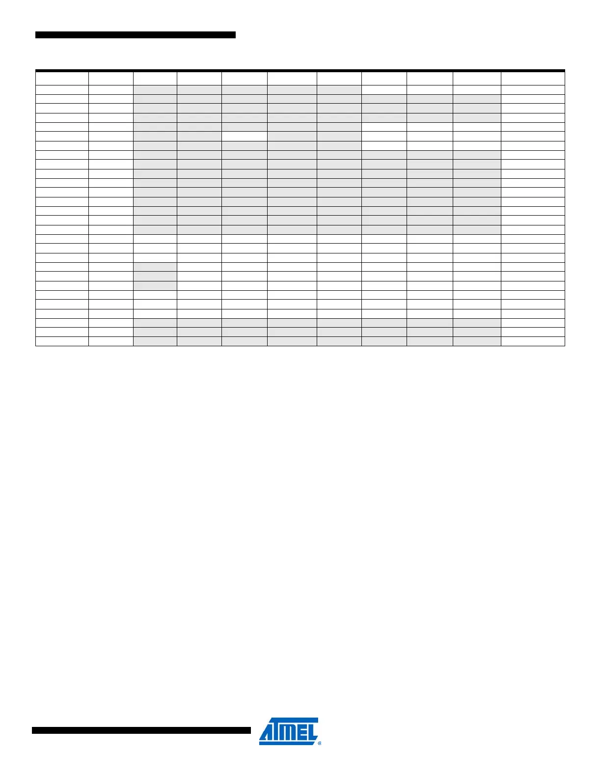
Note: 1. For compatibility with future devices, reserved bits should be written to zero if accessed. Reserved I/O memory addresses
should never be written.
2. I/O Registers within the address range 0x00 - 0x1F are directly bit-accessible using the SBI and CBI instructions. In these
registers, the value of single bits can be checked by using the SBIS and SBIC instructions.
3. Some of the Status Flags are cleared by writing a logical one to them. Note that, unlike most other AVRs, the CBI and SBI
instructions will only operate on the specified bit, and can therefore be used on registers containing such Status Flags. The
CBI and SBI instructions work with registers 0x00 to 0x1F only.
4. When using the I/O specific commands IN and OUT, the I/O addresses 0x00 - 0x3F must be used. When addressing I/O
Registers as data space using LD and ST instructions, 0x20 must be added to these addresses. The
ATmega48A/PA/88A/PA/168A/PA/328/P is a complex microcontroller with more peripheral units than can be supported
within the 64 location reserved in Opcode for the IN and OUT instructions. For the Extended I/O space from 0x60 - 0xFF in
SRAM, only the ST/STS/STD and LD/LDS/LDD instructions can be used.
5. Only valid for ATmega88A/88PA/168A/168PA/328/328P.
6. BODS and BODSE only available for picoPower devices ATmega48PA/88PA/168PA/328P
0x1B (0x3B) PCIFR – – – – – PCIF2 PCIF1 PCIF0
0x1A (0x3A) Reserved – – – – – – – –
0x19 (0x39) Reserved – – – – – – – –
0x18 (0x38) Reserved – – – – – – – –
0x17 (0x37) TIFR2 – – – – – OCF2B OCF2A TOV2 165
0x16 (0x36) TIFR1 – –ICF1 – – OCF1B OCF1A TOV1 141
0x15 (0x35) TIFR0 – – – – – OCF0B OCF0A TOV0
0x14 (0x34) Reserved – – – – – – – –
0x13 (0x33) Reserved – – – – – – – –
0x12 (0x32) Reserved – – – – – – – –
0x11 (0x31) Reserved – – – – – – – –
0x10 (0x30) Reserved – – – – – – – –
0x0F (0x2F) Reserved – – – – – – – –
0x0E (0x2E) Reserved – – – – – – – –
0x0D (0x2D) Reserved – – – – – – – –
0x0C (0x2C) Reserved – – – – – – – –
0x0B (0x2B) PORTD PORTD7 PORTD6 PORTD5 PORTD4 PORTD3 PORTD2 PORTD1 PORTD0 95
0x0A (0x2A) DDRD DDD7 DDD6 DDD5 DDD4 DDD3 DDD2 DDD1 DDD0 95
0x09 (0x29) PIND PIND7 PIND6 PIND5 PIND4 PIND3 PIND2 PIND1 PIND0 95
0x08 (0x28) PORTC
– PORTC6 PORTC5 PORTC4 PORTC3 PORTC2 PORTC1 PORTC0 94
0x07 (0x27) DDRC
– DDC6 DDC5 DDC4 DDC3 DDC2 DDC1 DDC0 94
0x06 (0x26) PINC – PINC6 PINC5 PINC4 PINC3 PINC2 PINC1 PINC0 94
0x05 (0x25) PORTB PORTB7 PORTB6 PORTB5 PORTB4 PORTB3 PORTB2 PORTB1 PORTB0 94
0x04 (0x24) DDRB DDB7 DDB6 DDB5 DDB4 DDB3 DDB2 DDB1 DDB0 94
0x03 (0x23) PINB PINB7 PINB6 PINB5 PINB4 PINB3 PINB2 PINB1 PINB0 94
0x02 (0x22) Reserved – – – – – – – –
0x01 (0x21) Reserved – – – – – – – –
0x0 (0x20) Reserved – – – – – – – –
Address Name Bit 7 Bit 6 Bit 5 Bit 4 Bit 3 Bit 2 Bit 1 Bit 0 Page