ATtiny10/11/12
4
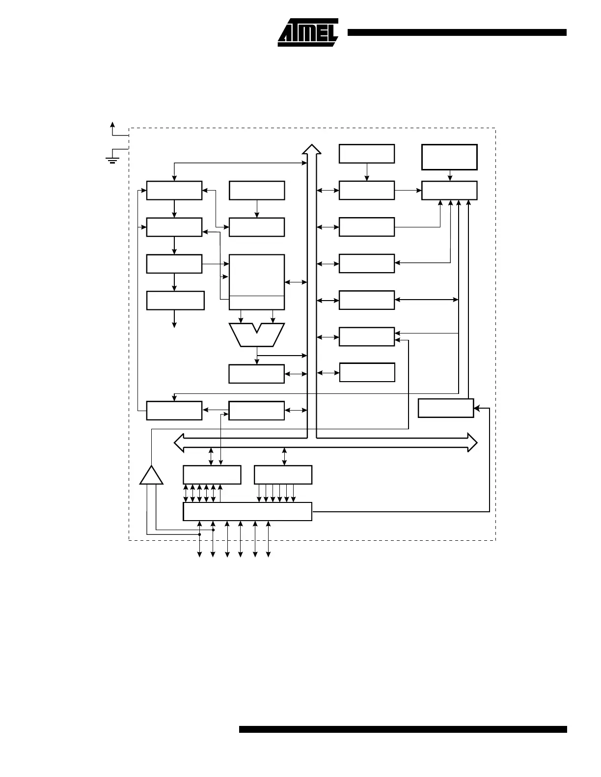
ATtiny12 Block Diagram
Figure 2. The ATtiny12 Block Diagram
The ATtiny12 provides the following features: 1K bytes of Flash, 64 bytes EEPROM, up to six general-purpose I/O lines,
32 general-purpose working registers, an 8-bit timer/counter, internal and external interrupts, programmable Watchdog
Timer with internal oscillator, and two software-selectable power-saving modes. The Idle Mode stops the CPU while allow-
ing the timer/counters and interrupt system to continue functioning. The Power-down Mode saves the register contents but
freezes the oscillator, disabling all other chip functions until the next interrupt or hardware reset. The wake-up or interrupt
on pin change features enable the ATtiny12 to be highly responsive to external events, still featuring the lowest power
consumption while in the power-down modes.
PROGRAM
COUNTER
INTERNAL
OSCILLATOR
WATCHDOG
TIMER
STACK
POINTER
PROGRAM
FLASH
HARDWARE
STACK
MCU CONTROL
REGISTER
GENERAL-
PURPOSE
REGISTERS
INSTRUCTION
REGISTER
TIMER/
COUNTER
INSTRUCTION
DECODER
DATA DIR.
REG. PORTB
DATA REGISTER
PORTB
PROGRAMMING
LOGIC
OSCILLATORS
TIMING AND
CONTROL
INTERRUPT
UNIT
MCU STATUS
REGISTER
STATUS
REGISTER
ALU
PORTB DRIVERS
PB0-PB5
VCC
GND
CONTROL
LINES
+
-
ANALOG
COMP
ARATOR
Z
8-BIT DATA BUS
EEPROM
SPI
INTERNAL
OSCILLATOR
CALIBRATED
 Loading...


