27
ATtiny15L
1187H–AVR–09/07
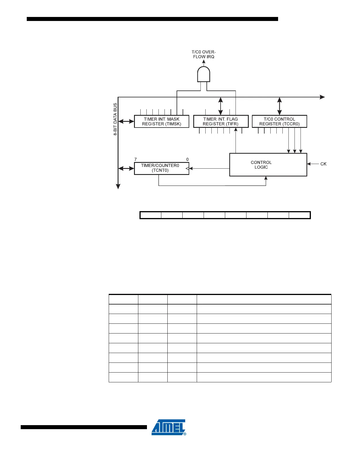
Figure 20. Timer/Counter0 Block Diagram
The Timer/Counter0 Control
Register – TCCR0
• Bits 7..3 – Res: Reserved Bits
These bits are reserved bits in the ATtiny15L and always read as zero.
• Bits 2, 1, 0 – CS02, CS01, CS00: Clock Select0, Bits 2, 1 and 0
The Clock Select0 bits 2, 1 and 0 define the prescaling source of Timer0.
The Stop condition provides a Timer Enable/Disable function. The prescaled CK modes
are scaled directly from the CK Oscillator clock. If the external pin modes are used for
Timer/Counter0, transitions on PB2/(T0) will clock the counter even if the pin is config-
ured as an output. This feature can give the user SW control of counting.
OCIE1A
TOIE1
TOIE0
TOV0TOV0
CS02
CS01
CS00
TOV1
OCF1A
T/C CLK SOURCE
Bit 76543210
$33 – – – – – CS02 CS01 CS00 TCCR0
Read/Write R R R R R R/W R/W R/W
Initial Value 0 0 0 0 0 0 0 0
Table 9. Clock 0 Prescale Select
CS02 CS01 CS00 Description
0 0 0 Stop, the Timer/Counter0 is stopped.
001CK
010CK/8
011CK/64
100CK/256
101CK/1024
1 1 0 External Pin T0, falling edge
1 1 1 External Pin T0, rising edge

 Loading...


