30-Oct-2020, Rev. 1.1
2.5.2.2 Layout Routing Guidelines
• The signals for each header follow FMC routing tolerances and guidelines.
Each of the P/N pairs have 50Ω single-ended impedance (100Ω differential)
with less than 10 mil skew between all P/N pairs on each header.
• There is less than 100 mil length skew across all bits in a bus or byte group,
including DQ and DQS pins in each bank.
• The dedicated analog signals, VP_0, VN_0, DXP and DXN are isolated from
other noisy signals by putting them at the end of the connector with a GND
isolating them from other signals. To minimize noise coupling, the
auxiliary/multi-use analog signals, IO_L*P_T1_AD*P/N_* use layer isolation,
pair routing and distance separation from other signals. Some of these are
shared with DQ byte groups above, in these cases, the DQ routing is more
important.
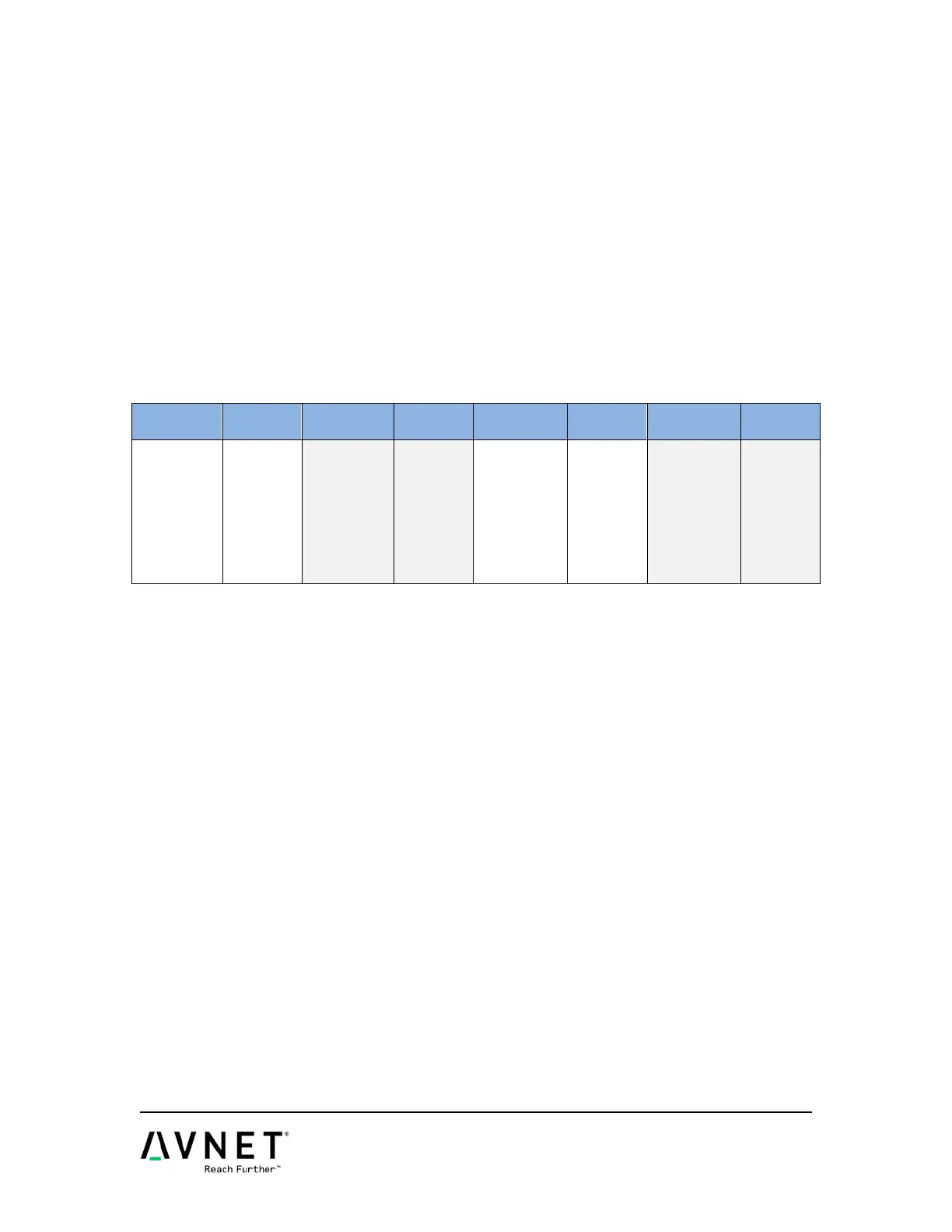
Table 14 – Data Byte Grouping
DQ[7:0]
B19
A20
D19
D20
E18
E19
DQ[15:8]
M17
M18
K19
J19
L16
L17
DQ[23:16]
H17
J18
H18
G18
J20
H20
DQ[31:24]
K14
J14
L14
L15
M14
M15
*As chosen by MIG 14.4 for a 7Z010-CLG400 package.