Chapter 3: Block Level Description
3-4 Advisor
®
Service Manual
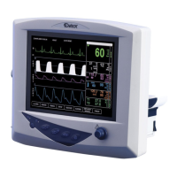
Main Board
The Main Board provides the majority of the Advisor Vital Signs Monitor functions: patient signal acquisition,
patient isolation (safety), user control interface, LCD display and backlight control, audio sound generator,
realtime clock and battery-backup memory, program memory, printer control, communications output, and an
independent self-powered critical failure alarm. The Advisor subsystems are detailed below.
Main Board - Microprocessor
The main processor (U21) is an ARM7, 32-bit RISC microprocessor, running from an external 14.7456 MHz spread-
spectrum clock source (U20, X3), but internally clocked at 77+MHz. The chip is a highly integrated controller
packaged in a low-pitch 176-pin LQFP package. On-chip integrated peripherals include an LCD video display
controller, memory controller, DMA controller, UART and synchronous serial interfaces, reset and power control,
PWM controllers, and a JTAG interface (J11). The microprocessor has an external 32-bit data bus and a 26-bit
address bus. The processor core runs on a 1.8 VDC supply (U17) and a 3.3 VDC supply (U15) to power input /
output (I/O).
Main Board - Reset System
The reset system is controlled by supervisory IC (U7). This IC monitors the main logic supply (Vcc), handles
switch-over to a lithium coin cell battery backup (BAT1), and provides a voltage comparator that is used to signal
the imminent loss of the main power source (UNSW_POWER). The supervisor IC and coin battery maintain a
backup power source (VRAM) to the Static Ram (SRAM) trend memory (U25) and the realtime clock IC (U2) at all
times.
Main Board - Clocks
The ARM7 microprocessor is clocked from an external 14.7456 MHz spread-spectrum clock source (U20, X3),
but internally is clocked-multiplied to 77+MHz. The spread-spectrum approach helps reduce EMC emissions
by spreading the emitted energy over a wider frequency band. Several other clock signals generated in the
main processor are derived from the main clock; the LCD display (LCD_CLK), SDRAM memory (SDCLK), and
Programmable Logic Device (PLD_CLK). This same 14.7456 MHz spread-spectrum clock source is used to clock
the Programmable Logic Device (U1). A 14.7456 MHz clock source is used to clock dual UART IC (U74). Realtime
clock controller (U2) uses its own 32.768 KHz watch crystal. The DSP uses a 18.432MHz clock.
Main Board - System Programmable Logic Device (PLD)
The Main Board consolidates the majority of its glue-logic in a Programmable Logic Device (U1). This PLD
is an Altera EPM3064A in a 100-pin LQFP package. The PLD is involved in the following functions: front
keypad interface (J8), rotary knob interface (J9), realtime clock (U2) serial communication, audio ON/OFF,
Communications Port & Smart Media interface (J20), memory bus control, rechargeable battery status, and
peripherals reset. The PLD can be in-circuit programmed through connector J1.