- 12 -
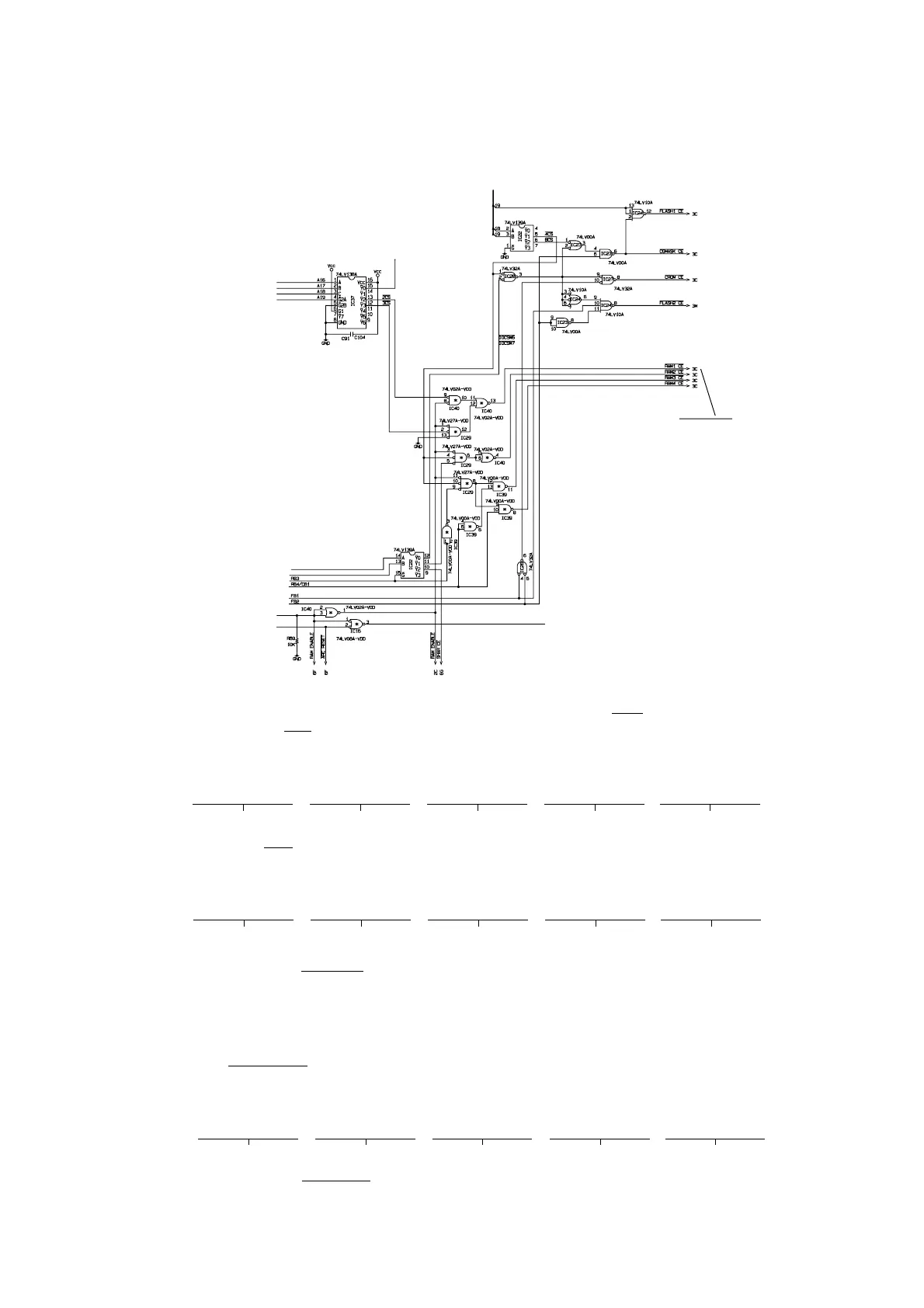
RB1
RB2
RB3
RB4/CB1
RAM enable
ARC RESET
RAM1 CE is for
RAM 1 chip enable signal.
RAM1 selection
The RAM1 is selected by the RAM enable signal "H" and the 2CS signal " L" of output pin
No.13 . The 2SC signal becomes "L" when the CPU address is as follows:
A19 A18 A17 A16 A15 A14 A13 A12 A11 A10 A9 A8 A7 A6 A5 A4 A3 A2 A1 A0
L L H L X X X X X X X X X X X X X X X X
2 X X X X
Therefore, the RAM1 CE will active when the CPU adress is from 20000H to 3FFFFH with
RAM enable signal "H".
Flash ROM1 selection
The Flash 1 CE will active by the IC25 output pin No.3. This is inverted signal of A19.
A19 A18 A17 A16 A15 A14 A13 A12 A11 A10 A9 A8 A7 A6 A5 A4 A3 A2 A1 A0
H L L L X X X X X X X X X X X X X X X X
8 X X X X
Therefore, the Flash1 CE will active when the CPU adress is from 80000H to FFFFFH.
Also, the 3SC signal becomes "L" when the CPU address is as follows:
A19 A18 A17 A16 A15 A14 A13 A12 A11 A10 A9 A8 A7 A6 A5 A4 A3 A2 A1 A0
L L H H X X X X X X X X X X X X X X X X
3 X X X X
6-4. Memory chip selection circuit
The RAM chip select signals made by the following circuit.
There are 4 chip enable signal lines for RAM selection and 3 chip enable signal lines for
Flash ROM selection (including Memory cassette).
 Loading...