- 38 -
12. LM2576HVT-5.0LB03
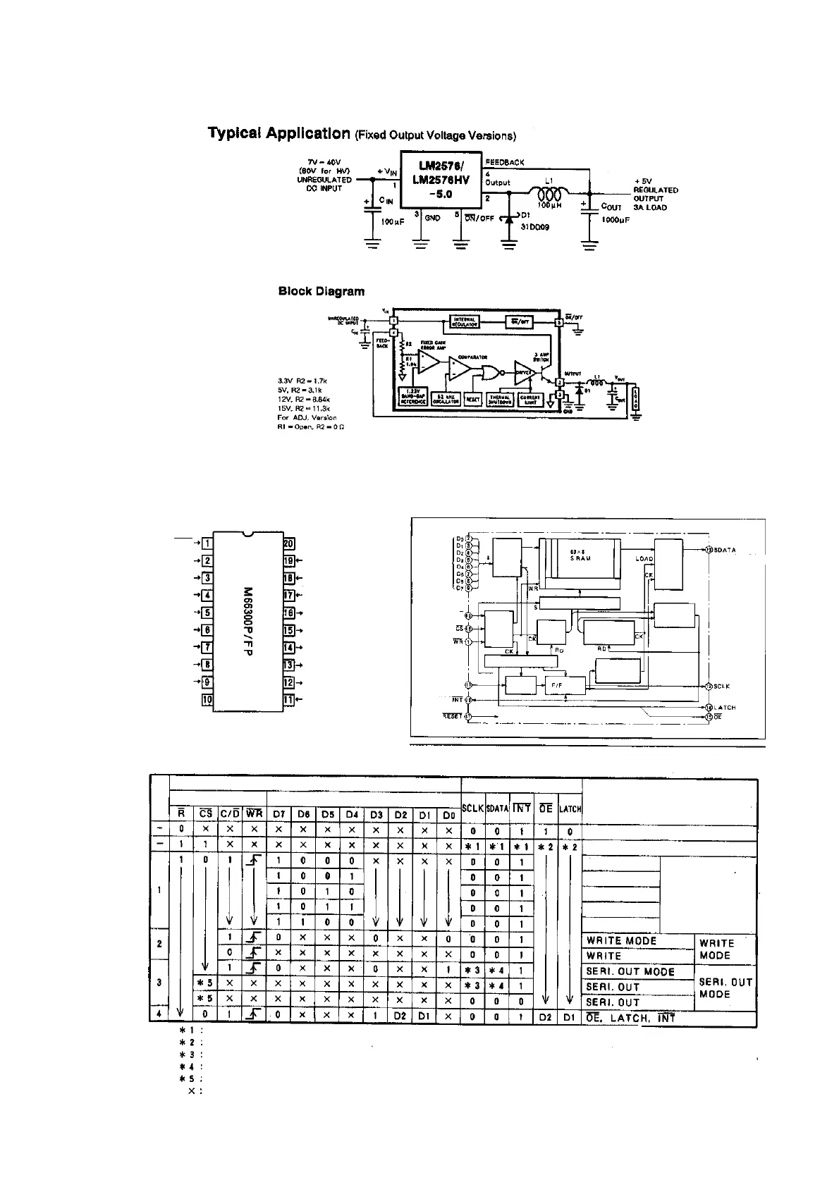
13. M66300FP-201
WR
D0
D1
D2
D3
D4
D5
D6
D7
GND
VCC
C/D
RESET
INT
OE
LATCH
SDATA
SCLK
CLK
BLOCK DIAGRAM
DATA PORT
SELEC-
TOR
BITS
DECODER
8bit shift
register
Output of shift register
Comparator
Selector
Counter for read
Counter
for write
Input
controller
Command register
Divider
Gate
bit/byte converter
Command/ Data
Input C/D
Chip select
Write input
Clock input CLK
Interrupt request
Reset input
Shift clock output
Latch output
Output enable output
Com-
mand
INPUT
Control input
Data input
OUTPUT
NOTE
Reset IC
Memory data is not changed.
Clock
1/2 clock
1/4 clock
1/8 clock
1/16 clock
Clock Divider will select when
the data D7 is "H".
/ Byte
SET
SET
/ Bit
Completed
Release
In the serial output mode, *3 and *4 are the same operation. In the othermode, output is not changed.
Output is not changed.
Selected the CLOCK divided pulse by the command 1 will be output by the high eadge of the Write signal.
SDATA(n) will be output by the low eadge of the (n-1) SCLK pulse.
When WR is "0", it is "0". When WR is "1", do not care.
Do not care.
NOTE :
FUNCTION TABLE
 Loading...