Schematic Diagrams
B - 1
B.Schematic Diagrams
Appendix B: Schematic Diagrams
Table B - 1
SCHEMATIC
DIAGRAMS
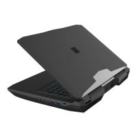
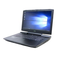
This appendix has circuit diagrams of the P650HS(-G) / P651HS(-G) notebook’s PCB’s. The following table indicates
where to find the appropriate schematic diagram.
Diagram - Page Diagram - Page Diagram - Page Diagram - Page
System Block Diagram - Page B - 2 Frame Buffer Partition C_D - Page B - 26 M.2 3G/LTE - Page B - 50 VCC_Core & VCCSA - Page B - 74
Processor 1/7 - Page B - 3 GPU Decoupling 1 - Page B - 27 Realtek ALC898 - Page B - 51 VCore Output Stage - Page B - 75
Processor 2/7 - Page B - 4 GPU Decoupling 2 - Page B - 28 TPA2008D2 - Page B - 52 VCCGT - Page B - 76
Processor 3/7 - Page B - 5 Straps & XTAL - Page B - 29 Subwoofer - Page B - 53 VCCGT Output Stage - Page B - 77
Processor 4/7 - Page B - 6 IFP I/O Interface - Page B - 30 AR_TBT - Page B - 54 Audio Board P65_ESS_A 1/3 - Page B - 78
Processor 5/7 - Page B - 7 Misc - GPIO, I2C and ROM - Page B - 31 AR_Power - Page B - 55 Audio Board P65_ESS_A 2/3 - Page B - 79
Processor 6/7 - Page B - 8 NVIDIA Power Sequence - Page B - 32 TPS65982 - Page B - 56 Audio Board P65_ESS_A 3/3 - Page B - 80
Processor 7/7 - Page B - 9 GPIO Level Shift - Page B - 33 TPS65982-1 - Page B - 57 Audio Board P67_3DAMP_E - Page B - 81
DDR CHA SO-DIMM_0 - Page B - 10 GPU NVVDD, FBVDDQ - Page B - 34 AR_Conn Type A/C - Page B - 58 P650RS Power Board - Page B - 82
DDR CHA SO-DIMM_1 - Page B - 11 GPU GND - Page B - 35 TPM, CCD, TP - Page B - 59 P650RS HDD Board - Page B - 83
DDR CHB SO-DIMM_0 - Page B - 12 PCH 1/9 - Page B - 36 Fan, LID, KB LED - Page B - 60 P650RS LED Board - Page B - 84
DDR CHB SO-DIMM_1 - Page B - 13 PCH 2/9 - Page B - 37 Connector - Page B - 61 P650RS FP Board - Page B - 85
Panel, Inverter - Page B - 14 PCH 3/9 - Page B - 38 DDR 1.2V / 0.6VS - Page B - 62 P650RS Click Board - Page B - 86
Mini DP Port E - Page B - 15 PCH 4/9 - Page B - 39 VDD3, VDD5 - Page B - 63 P650RS USB Board 1/3 - Page B - 87
Mini DP Port F + PS8330B - Page B - 16 PCH 5/9 - Page B - 40 5V, 5VS, 3.3V, 3.3VS, 3.3VA - Page B - 64 P650RS USB Board 2/3 - Page B - 88
HDMI - Page B - 17 PCH 6/9 - Page B - 41 Power 1.0V, VCCIO - Page B - 65 P650RS USB Board 3/3 - Page B - 89
VGA PCI Express - Page B - 18 PCH 7/9 - Page B - 42 AC_In, Charger - Page B - 66 P670RS LED Board - Page B - 90
VGA Frame Buffer Partition - Page B - 19 PCH 8/9 - Page B - 43 1.0DX_VCCSTG/VCCSFR_OC/2.5V - Page B - 67 P670RS USB Board 1/2 - Page B - 91
Frame Buffer Partition A - Page B - 20 PCH 9/9 - Page B - 44 1V8_RUN/AON, NV3V3 - Page B - 68 P670RS USB Board 2/2 - Page B - 92
Frame Buffer Partition B - Page B - 21 KBC IT8587 - Page B - 45 NVVDD Phase 1 & 2 - Page B - 69
Frame Buffer Partition A_B - Page B - 22 RGB KB Only - Page B - 46 NVVDD Phase 3~4 - Page B - 70
GPU Frame Buffer Partition - Page B - 23 USB Charger - Page B - 47 NVVDDS - Page B - 71
Frame Buffer Partition C - Page B - 24 M.2 WiGig/WLAN + BT - Page B - 48 PEX_VDD - Page B - 72
Frame Buffer Partition D - Page B - 25 M.2 PCIE4X SSD - Page B - 49 FBVDDQ - Page B - 73
Version Note
The schematic dia-
grams in this chapter
are based upon ver-
sion 6-7P-P65SB-008.
If your mainboard (or
other boards) are a lat-
er version, please
check with the Service
Center for updated di-
agrams (if required).