Schematic Diagrams
B - 1
B.Schematic Diagrams
Appendix B: Schematic Diagrams
Table B - 1
SCHEMATIC
DIAGRAMS
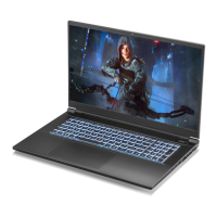
This appendix has circuit diagrams of the PD70PNT / PD70PNN / PD70PNR / PD71PNT / PD71PNN / PD71PNR
notebook’s PCB’s. The following table indicates where to find the appropriate schematic diagram.
Diagram - Page Diagram - Page Diagram - Page Diagram - Page
System Block Diagram - Page B - 2 Frame Buffer Partition B - Page B - 26 PS8802 - Page B - 50 FBVDD - Page B - 74
Processor 1/13 - Page B - 3 Frame Buffer Partition C_D - Page B - 27 PD Controller IT8851 - Page B - 51 AC_In, Charger - Page B - 75
Processor 2/13 - Page B - 4 Frame Buffer Partition C - Page B - 28 LAN RTL8111H - Page B - 52 15” Audio Board 1 - Page B - 76
Processor 3/13 - Page B - 5 Frame Buffer Partition C - Page B - 29 EC ITE5570 - Page B - 53 15” Audio Board 2 - Page B - 77
Processor 4/13 - Page B - 6 Frame Buffer Partition D - Page B - 30 M.2 PCIE Gen4 SSD - Page B - 54 17” Audio Board 1 - Page B - 78
Processor 5/13 - Page B - 7 Frame Buffer Partition D - Page B - 31 M.2 WLAN+BT - Page B - 55 17” Audio Board 2 - Page B - 79
Processor 6/13 - Page B - 8 GPU PWR & GND - Page B - 32 TPM, Screw - Page B - 56 LED Board PD50 - Page B - 80
Processor 7/13 - Page B - 9 GPU PWR & GND - Page B - 33 Per Key LED KB - Page B - 57 Power Board PD50 - Page B - 81
Processor 8/13 - Page B - 10 GPU Decoupling - Page B - 34 NB Connector - Page B - 58 LED Board PD70 - Page B - 82
Processor 9/13 - Page B - 11 GPU IFPAB DPIIM - Page B - 35 Backlight KB - Page B - 59 Power Board PD70 - Page B - 83
Processor 10/13 - Page B - 12 GPU IFPCD DPIIM - Page B - 36 Card Connector - Page B - 60 Power Sequence - Page B - 84
Processor 11/13 - Page B - 13 GPU IFPE Mictor - Page B - 37 5V, 5VS, 3.3V, 3.3VS - Page B - 61
Processor 12/13 - Page B - 14 GPU IFPF USB-C DP - Page B - 38 VDD3, VDD5 - Page B - 62
Processor 13/13 - Page B - 15 Output Power Measurement - Page B - 39 3.3VA, NV3V3 - Page B - 63
DDR4 CHA SO-DIMM_0 - Page B - 16 GPU GPIO, Fan, JTAG - Page B - 40 MP2964 Controller - Page B - 64
DDR4 CHB SO-DIMM_0 - Page B - 17 GPU ROM, Straps - Page B - 41 VCore Output Stage - Page B - 65
Panel, Inverter - Page B - 18 GPU XTAL - Page B - 42 VCCGT - Page B - 66
Mini DP Port - Page B - 19 eDP 2-to-1 PS8461 SW - Page B - 43 DDR 1.2V, 0.6VS - Page B - 67
HDMI - Page B - 20 Audio Codec - Page B - 44 VCCIN AUX - Page B - 68
PCI Express - Page B - 21 Smart AMP - Page B - 45 1.8VA, VCCST - Page B - 69
Frame Buffer Partition A_B - Page B - 22 TBT Retimer 1/2 - Page B - 46 PEX_VDD, 1.2VS, 1V8_AON - Page B - 70
Frame Buffer Partition A - Page B - 23 TBT Retimer 2/2 - Page B - 47 NVVDD 1 - Page B - 71
Frame Buffer Partition A - Page B - 24 TPS65987D - Page B - 48 NVVDD 2 - Page B - 72
Frame Buffer Partition B - Page B - 25 Card Reader - Page B - 49 FBVDD - Page B - 73
Version Note
The schematic dia-
grams in this chapter
are based upon version
6-7P-PD507-002. If your
mainboard (or other
boards) are a later ver-
sion, please check with
the Service Center for
updated diagrams (if re-
quired).