Chapter 7 Option Cards | VFD-ED
7-3-2 Terminal Function
Terminals Descriptions
TB1
Vin
Voltage input: (to adjust the output voltage amplitude of the push
pull pulse)
Max. input voltage: 24 V
DC
Max. input current: 30 mA
A/O, B/O
Push-pull pulse output signal
Max. output frequency: 50 kHz
GND Common power input/signal output terminal
AO, /AO, BO, /BO
Output signal for the line driver frequency division.
Line driver RS422
Max. input frequency: 100 kHz
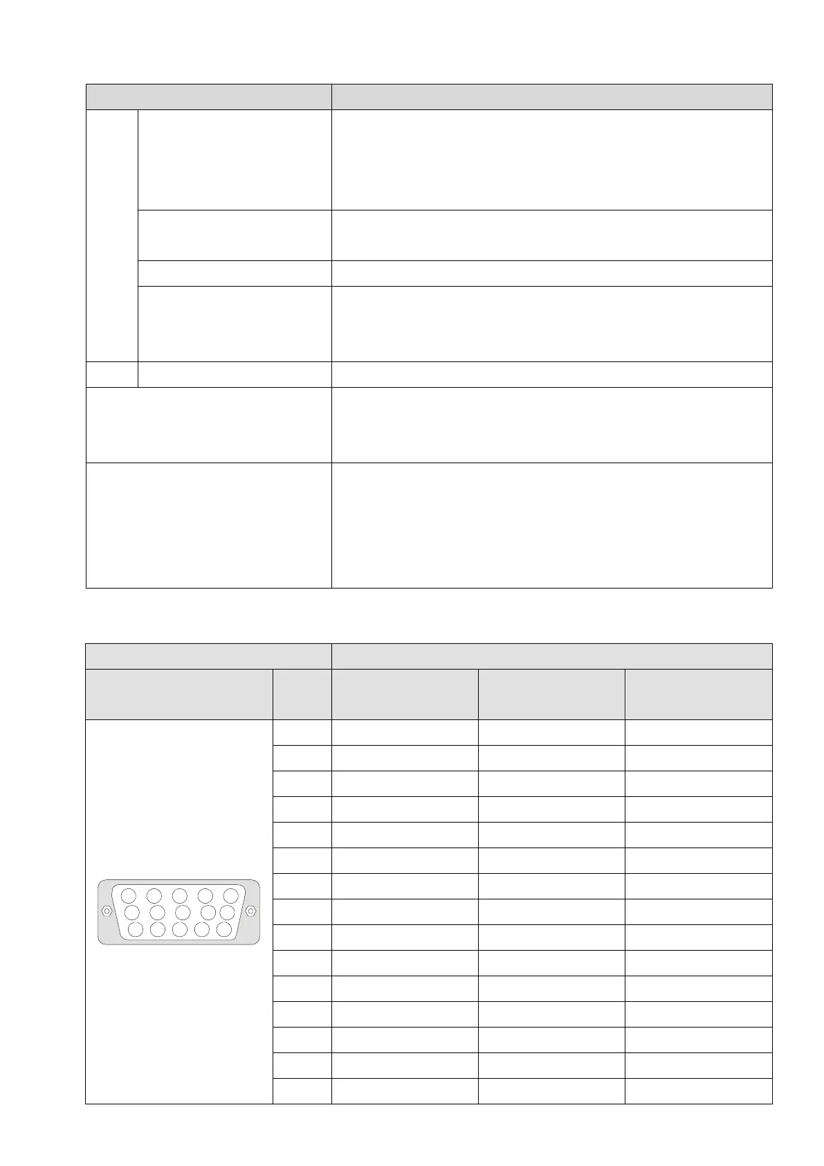
J3 (D-SUB female connector) Encoder signal input terminal
SW1
Frequency division output power terminal selection
INP: Power supplied by PG card
EXP: Power from an external source
SW2
Encoder’s voltage output terminal (Up)
NOTE: Modify the terminal output voltage by switching the
direction of the SW2 DIP switch on the PG card.
5V: 5 V
DC
8V: 8 V
DC
EMED-PGHSD-3 (Terminal J3) pin definitions depend on the encoder type
J3 No.
Heidenhain
Heidenhain
HIPERFACE
○
R
5
4
3
2
1
10 9 8 7
6
15
14
13 12
11
1
2
3
4
5
6
7
8
9
10
11
12
13
14
15
 Loading...