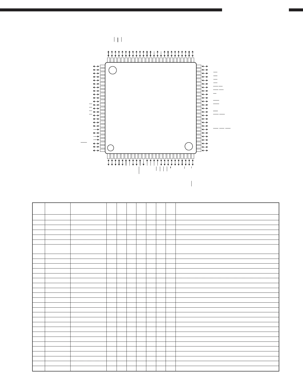
22
AVR-5803/AVC-A1SR
1 P94 SPIDS2 O C — — — Z H DSP2 serial control terminal (ADSP21161L)
2 P93 CS SUB O C — — — Z L 1394 comm. control terminal
3 P92/SOUT3 TxD SUB O C — — — Z L 1394 comm. control terminal
4 P91/SIN3 RxD SUB O C — — — Z L 1394 comm. control terminal
5 P90/CLK3 CLK SUB O C — — — Z L 1394 comm. control terminal
6 BYTE BYTE ———————GND (Ext. data bus bit width switching, L: 16bit)
7 CNVCS CNVSS ———————Single-chip/Microprocessor mode switching
(L: Single-chip, H: Rewrite boot program)
8 P87 ROM_RST2 O C — — Od Z L Memory reset for DSP2 (L: Reset)
9 P86 ROM_RST1 O C — — Od Z L Memory reset for DSP1 (L: Reset)
10 RESET _RESET I — Lv Iu — L — Reset input
11 XOUT X1 O ——————Oscillator connection
12VSS VSS ———————GND
13XIN X2 I ——————Oscillator connection
14VCC VCC ———————+3V
15 P85/NMI _NMI I ——————Not used (Fixed to H)
16 P84/INT2 _INT1 I —
E↓&L
— — Z — DIR1 control terminal (LC89057W-E)
17 P83/INT1 _ACK I —
E↓&L
—Eu Z —
Main/Sub-mcom comm. control input (ACK from mcom L return)
18 P82/INT0 _B. DOWN I —
E↓&L
— Eu Z — Power down detect (L: Down)
19 P81 ADC RESET 0 C — — — Z H A/D control terminal (L: Reset)
20 P80 DIGITAL POWER 0 C — — — Z L Digital power on/off switching
21 P77 DAC DIF 0 C — — — Z L DAC deferential used: H
22 P76 OSR1 0 C — — — Z H A/D control terminal (PCM1804), H:192kHz
23 P75 OSR2 0 C — — — Z L A/D control terminal (PCM1804), H:96kHz
24 P74 DIR CE 0 C — — — Z L
DIR control terminal (LC89057W-E), control chip enable output
25 P73/CTS2 DIR_RST 0 C — — — Z L DIR control terminal (LC89057W-E), L: Reset
26 P72/CLK2 DIR CLK 0 C — — — Z L DIR control terminal (LC89057W-E), control clock output
27 P71/RXD2 DIR DIN 0 N — — Eu Z L DIR control terminal (LC89057W-E), control data output
28 P70/TXD2 DIR DOUT I — Lv — — Z — DIR control terminal (LC89057W-E), control data input
29 P67/TXD1 TxD O C — — — Z L Data send to external
30 P66/RXD1 RxD I — Lv — — Z — Data receive from external
31 P65/CLK1 DACMC O C — — — Z L DAC control terminal (PCM1738)
Det FunctionI/O Type Ext Int Res Init
Pin
No.
Pin Name Symbol
P94/DA1/TB4IN
P13/D11
P93/DA0/TB3IN
P14/D12
P92/TB2IN/SOUT3
P1
5/D13/INT3
P91/TB1IN/SIN3
P1
6D14/INT4
P90/TB0IN/CLK3
P1
7/D15/INT5
BYTE
P2
0/A0(/D0/−)
CNVSS
P21/A1(/D1/D0)
P87/XCIN
P22/A2(/D2/D1)
P86/XCOUT
P23/A3(/D3/D2)
RESET
P2
4/A4(/D4/D3)
XOUT
P25/A5(/D5/D4)
VSS
P26/A6(/D6/D5)
XIN
P27/A7(/D7/D6)
VCC
VSS
P85/NMI
P3
0/A8(/−/D7)
P84/INT2
VCC
P83/INT1
P31/A9
P82/INT0
P32/A10
P81/TA4IN/U
P3
3/A11
P80/TA4OUT/U
P3
4/A12
P77/TA3IN
P35/A13
P76/TA3OUT
P36/A14
P75/TA2IN/W
P3
7/A15
P74/TA2OUT/W
P4
0/A16
P73/CTS2/RTS2/TA1IN/V
1
75
2
74
3
73
4
72
5
71
6
70
7
69
8
68
9
67
10
66
11
65
12
64
13
63
14
62
15
61
16
60
17
59
18
58
19
57
20
56
21
55
22
54
23
53
24
52
25
51
P41/A17
P12/D10
P42/A18
P11/D9
P43/A19
P10/D8
P44/CS0
P07/D7
P45/CS1
P06/D6
P46/CS2
P05/D5
P47/CS3
P04/D4
P50/WRL/WR
P03/D3
P51/WRH/BHE
P02/D2
P52/RD
P01/D1
P53/BCLK
P00/D0
P54/HLDA
P107/AN7/KI3
P55/HOLD
P106/AN6/KI2
P56/ALE
P105/AN5/KI1
P57/RDY/CLKOUT
P104/AN4/KI0
P60/CTS0/RTS0
P103/AN3
P61/CLK0
P102/AN2
P62/RXD0
P101/AN1
P63/TXD0
AVSS
P64/CTS1/RTS1/CTS0/CLKS1
P100/AN0
P65/CLK1
VREF
P66/RXD1
AVCC
P67/TXD1
P97/ADTRG/SIN4
P7
0/TXD2/SDA/TA0OUT
P96/ANEX1/SOUT4
P7
1/RXD2/SCL/TA0IN/TB5IN
P95/ANEX0/CLK4
76
50
77
49
78
48
79
47
80
46
81
45
82
44
83
43
84
42
85
41
86
40
87
39
88
38
89
37
90
36
91
35
92
34
93
33
94
32
95
31
96
30
97
29
98
28
99
27
100
26
P7
2/CLK2/TA1OUT/V
TOP VIEW
M30620FCMGP Terminal Function
M30620FCMGP (IC701) (SUB)
 Loading...