PCM1690 (FRONT CNT : IC301)
Pin Function
TERMINAL
I/O
PULL-
DOWN
5-V
TOLERANT
DESCRIPTION
NAME PIN
RSV2 1 — — — Reserved, tied to analog ground
RSV1 2 — — — Reserved, left open
RSV2 3 — — — Reserved, tied to analog ground
RSV1 4 — — — Reserved, left open
RSV2 5 — — — Reserved, tied to analog ground
LRCK 6 I Yes No Audio data word clock input
BCK 7 I Yes No Audio data bit clock input
DIN1 8 I No No Audio data input for DAC1 and DAC2
DIN2 9 I No No Audio data input for DAC3 and DAC4
DIN3 10 I No No Audio data input for DAC5 and DAC6
DIN4 11 I No No Audio data input for DAC7 and DAC8
VDD 12 — — — Digital power supply, +3.3 V
DGND 13 — — — Digital ground
SCKI 14 I No Yes System clock input
RST 15 I Ye s Yes Reset and power-down control input with active low
ZERO1 16 O No No Zero detect ag output 1
ZERO2 17 O No No Zero detect ag output 2
AMUTEI 18 I No Ye s Analog mute control input with active low
AMUTEO 19 O No Yes Analog mute status output(1) with active low
MD/SDA/DEMP 20 I/O No Ye s Input data for SPI, data for I2C(1), de-emphasis control for hardware control mode
MC/SCL/FMT 21 I No Yes Clock for SPI, clock for I2C, format select for hardware control mode
MS/ADR0/RSV 22 I Ye s Ye s
Chip Select for SPI, address select 0 for I2C, reserve (set low) for hardware control
mode
TEST/ADR1/RSV 23 I/O No Ye s
Test (factory use, left open) for SPI, address select 1 for I2C, reserve (set low) for
hardware control mode
MODE 24 I No No Control port mode selection. Tied to VDD: SPI, left open: H/W mode, tied to DGND: I2C
VCC1 25 — — — Analog power supply 1, +5 V
VCOM 26 — — — Voltage common decoupling
AGND1 27 — — — Analog ground 1
RSV2 28 — — — Reserved, tied to analog ground
VOUT8+ 29 O No No Positive analog output from DAC8
VOUT8- 30 O No No Negative analog output from DAC8
VOUT7+ 31 O No No Positive analog output from DAC7
VOUT7- 32 O No No Negative analog output from DAC7
VOUT6+ 33 O No No Positive analog output from DAC6
VOUT6- 34 O No No Negative analog output from DAC6
VOUT5+ 35 O No No Positive analog output from DAC5
VOUT5- 36 O No No Negative analog output from DAC5
VOUT4+ 37 O No No Positive analog output from DAC4
VOUT4- 38 O No No Negative analog output from DAC4
VOUT3+ 39 O No No Positive analog output from DAC3
VOUT3- 40 O No No Negative analog output from DAC3
VOUT2+ 41 O No No Positive analog output from DAC2
VOUT2- 42 O No No Negative analog output from DAC2
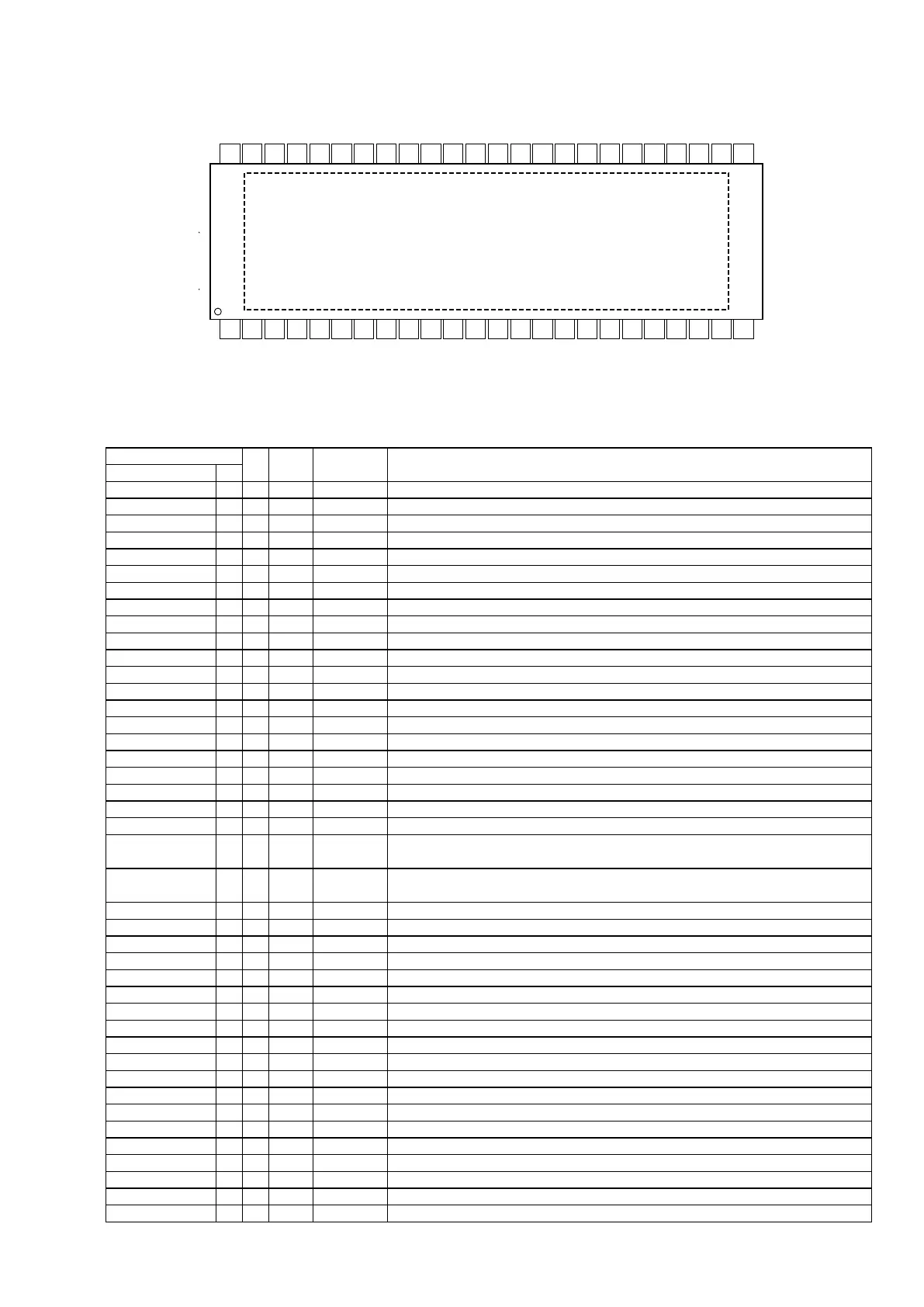
1
2
3
4
5
6
7
8
9
10
11
12
13
14
15
16
17
18
19
20
21
22
23
24
48
47
46
45
44
43
42
41
40
39
38
37
36
35
34
33
32
31
30
29
28
27
26
25
RSV2
VCC2
AGND2
RSV2
VOUT1
VOUT2
VOUT3
VOUT4
VOUT5
VOUT6
VOUT7
VOUT8
RSV2
AGND1
VCOM
VCC1
RSV2
RSV1
RSV2
RSV1
RSV2
LRCK
BCK
DIN1
DIN2
DIN3
DIN4
VDD
DGND
SCKI
RST
ZERO1
ZERO2
AMUTEI
AMUTEO
MD/SDA/DEMP
MC/SCL/FMT
MS/ADR0/RSV
MODE
PCM1690
ThermalPad
PCM1690
SBAS448A– OCTOBER 2008–REVISED JANUARY 2009..............................................................................................................................................
www.ti.com
DCA PACKAGE
HTSSOP-48 (12 mm x 8 mm)
(TOP VIEW)
TERMINAL FUNCTIONS
TERMINAL
PULL- 5-V
NAME PIN I/O DOWN TOLERANT DESCRIPTION
RSV2 1 — — — Reserved, tied to analog ground
RSV1 2 — — — Reserved, left open
RSV2 3 — — — Reserved, tied to analog ground
RSV1 4 — — — Reserved, left open
RSV2 5 — — — Reserved, tied to analog ground
LRCK 6 I Yes No Audio data word clock input
BCK 7 I Yes No Audio data bit clock input
DIN1 8 I No No Audio data input for DAC1 and DAC2
DIN2 9 I No No Audio data input for DAC3 and DAC4
DIN3 10 I No No Audio data input for DAC5 and DAC6
DIN4 11 I No No Audio data input for DAC7 and DAC8
6 Submit Documentation Feedback Copyright © 2008–2009, Texas Instruments Incorporated
Product Folder Link(s): PCM1690
173
 Loading...