Do you have a question about the Denon AVR-X4100W and is the answer not in the manual?
Crucial safety check before returning the unit to the customer.
General cautions and instructions to heed during servicing and inspection.
Highlights critical safety components that require specific replacement parts.
ESD precautions for the user: wear a grounding band to remove static electricity.
ESD precautions for the workbench: use a conductive sheet with proper grounding.
Details about the audio amplifier, rated output, and dynamic power.
Details about standard and component video connectors and frequency response.
Specifications for FM and AM reception frequency ranges and sensitivity.
Details wireless LAN standards, security, frequency band, and channels.
Details Bluetooth communication system, transmission power, range, and profiles.
Power supply requirements, power consumption in various modes, and design change notice.
Procedure for unit initialization after microcomputer or digital PCB replacement.
Information on necessary jigs (extension cable kit) for PCB repair.
Details the proceeding and steps for removing the front panel assembly.
Details the proceeding and steps for removing the radiator assembly.
Details the proceeding and steps for removing the digital PCB.
Details the proceeding for removing the video PCB assembly.
Details the proceeding for removing the input PCB.
Details the proceeding and steps for removing the speaker PCB.
Mentions SMPS PCB removal instructions.
Mentions Trans Power removal instructions.
Describes the buttons used to enter special modes and their functions.
Describes the purpose of the version display mode.
Steps to start the version display mode and show firmware information.
Outlines the order of information displayed in the version list.
Details the error when firmware information does not match region settings.
Details the error when there is no reply from SUB u-COM.
Details the error occurring in Loopback Test of DDR memory.
Details the error occurring in Loopback Test of DDR memory for GUI firmware.
Details the error displayed if there is no response from the DIR.
Details the error related to DSP flag status during boot or data reading.
Details the error occurred in a checksum of the EEPROM.
Explains how to turn the PANEL LOCK and REMOTE LOCK modes on and off.
Steps to enter the PANEL/REMOTE LOCK selection mode.
How modes are displayed and selected using cursor and enter buttons.
Select diagnostic mode, protection history display mode, or 232C standby clear mode.
Steps to enter the service-related operation modes.
How to navigate and select the desired service mode.
How to exit the service-related operation modes.
Purpose of the diagnostic mode for confirming problem paths and executing a path check.
Steps to start the diagnostic mode and check video and audio paths.
How to exit the diagnostic mode by pressing the power button.
How to switch between video items and audio items.
Details audio paths and settings for confirmation.
Explains how this mode records and displays activated protection events.
Steps to enter the protection history display mode.
How protection events (ASO, DC, THERMAL, CURRENT) are displayed.
Describes two ways to clear the protection history.
Explains power LED indications for protection status.
Switches from 232C standby mode to normal standby mode.
Steps to enter the 232C standby clear mode.
Purpose of this mode: displays operating time, power on count, and protection counts.
Steps to enter the operation info mode.
How information is displayed: operating time, power count, protection counts.
This mode enables changing the reception STEP of the analog tuner.
Steps to enter the tuner step mode.
Information displayed in the tuner step mode.
Allows operation of only the desired AV receiver when multiple are in the same room.
Steps to enter the remote ID setup mode.
How to set the remote ID using quick select buttons.
Steps to set the remote control unit's ID.
Allows power to be turned on without activating protections.
Steps to enter the protection pass mode.
Explains how to restart the CX870/CY920 after hangup.
Steps to perform the CX870/CY920 reboot.
Lists items initialized: Favorites, Quick Select, Presets, etc.
Steps to enter the initialization mode.
Details on connecting jigs for the digital PCB repair.
Lists items needed for jig connection, such as extension kits.
Outlines the steps for connecting expansion cables and removing PCBs.
General procedure for updating firmware.
Instructions for updating firmware via USB memory.
Preparation steps for USB connection, including format and connection guidelines.
Steps for unzipping the firmware file and copying it to the USB drive.
Instruction on inserting the USB drive into the unit's USB port.
Steps to initiate the firmware update process.
Shows the message displayed on the unit during the USB update.
Displays shown upon successful completion of the firmware update.
Critical precautions to follow during firmware updates.
Mode used when the unit cannot be recovered, forcing USB update.
Steps to activate the forced USB device write mode.
Table detailing USB update error codes, their descriptions, and coping strategies.
Instructions to verify the firmware version after the update process.
System requirements for network connection for firmware updates.
Steps to check for and perform firmware updates via DPMS.
Important precautions for firmware updates, including network and power considerations.
Table detailing DPMS update error codes, their descriptions, and coping strategies.
Instructions to check the firmware version after the update process.
Specific procedure for adjusting the idling current.
Steps to prepare for the adjustment, including equipment and settings.
Detailed steps for performing the idling current adjustment.
Explains how sound modes map to channel outputs based on speaker configuration.
Troubleshooting steps for power-related issues.
Flowchart for diagnosing power-on failures.
Procedure for checking and replacing fuses.
Flowchart for diagnosing HDMI output failures.
Flowchart for diagnosing no audio output.
Steps to diagnose network connection problems.
Printed wiring board layout for the digital PCB.
Printed wiring board layout for the CX870 MIDDLE PCB.
Printed wiring board layout for the Bluetooth module.
Identifies test points on the input PCB.
Printed wiring board layout for the guide FFC.
Printed wiring board layout for the front CNT PCB.
Printed wiring board layout for the front HDMI FFC cable.
Printed wiring board layout for the head phone part.
Printed wiring board layout for the FHDMI part.
Printed wiring board layout for the AMP PCB.
Printed wiring board layout for the guide.
Printed wiring board layout for the fuse PCB.
Schematic for digital interconnections between components.
Schematic for digital power supply circuits.
Schematic for the main CPU and its connections.
Schematic for the sub CPU and its connections.
Schematic for CPU level changing circuits.
Schematic for the DIR (Digital Interface Receiver).
Schematic for the Audio PLD.
Schematic for the first DSP.
Schematic for the second DSP.
Schematic for the third DSP.
Schematic for the fourth DSP.
Schematic for the ADC (Analog-to-Digital Converter).
Schematic for ZONE DAC circuits.
Schematic for the CY920 network module.
Schematic for the video decoder.
Schematic for the HDMI switch (SW2).
Schematic for the HDMI switch (SW1).
Schematic for Video Signal Processing, IP Scaler, and OSD.
Schematic for the Video PLD.
Schematic for HDMI transmitter and scaler.
Schematic for the adapter module.
Schematic for the Bluetooth module.
Schematic for the input board.
Schematic for the pre-output circuits.
Schematic for the front HDMI input.
Schematic for the video circuits.
Schematic for RC-5 and MX-PORT connections.
Schematic for RS232C and trigger connections.
Schematic for connection A.
Schematic for connection B.
Schematic for the main DAC1.
Schematic for the main DAC2.
Schematic for the speaker output stage.
Schematic for voltage regulators and tuner circuits.
Schematic for the first 7-channel amplifier stage.
Schematic for the second 7-channel amplifier stage.
Schematic for the front panel circuits.
Schematic for the SMPS (Switch Mode Power Supply).
Details of ICs used in the unit.
Terminal functions for the R5F56108VNFP IC.
Block diagram for the PCM9211 IC.
Lists terminal functions for the ADSP21487KSWZ3B.
Explains the purpose of each pin.
Block diagram of the MX25L1606EM2I-12G.
Lists terminal functions for PCM510x series devices.
Block diagram of the PCM510x audio DAC.
Details the pin functions for the AK5358BET ADC.
Lists terminal functions for the PCM1690 DAC.
Block diagram of the PCM1690 DAC.
Shows the block diagram and pin configuration of the R2A15220FP.
Shows the block diagram and pin configuration of the R2A15218FP.
Block diagram of the NJW1194A audio IC.
Pin connections for the FL display module.
Grid assignment for the FL display segments.
Lists semiconductor components for the front PCB.
Lists resistor components for the front PCB.
Lists capacitor components for the front PCB.
Lists other miscellaneous parts for the front PCB.
Lists semiconductor components for the video PCB.
Lists resistor components for the video PCB.
Lists capacitor components for the video PCB.
Lists other miscellaneous parts for the video PCB.
Lists semiconductor components for the 7CHAMP PCB.
Lists resistor components for the 7CHAMP PCB.
Lists capacitor components for the 7CHAMP PCB.
Lists semiconductor components for the SPK PCB.
Lists resistor components for the SPK PCB.
Lists capacitor components for the SPK PCB.
Lists other miscellaneous parts for the SPK PCB.
Lists semiconductor components for the F_HDMI PCB.
Lists resistor components for the F_HDMI PCB.
Lists capacitor components for the F_HDMI PCB.
Lists other miscellaneous parts for the F_HDMI PCB.
Lists semiconductor components for the SMPS PCB.
Lists resistor components for the SMPS PCB.
Lists capacitor components for the SMPS PCB.
Lists other miscellaneous parts for the SMPS PCB.
Lists semiconductor components for the CX870 CONNECTOR PCB.
Lists resistor components for the CX870 CONNECTOR PCB.
Lists capacitor components for the CX870 CONNECTOR PCB.
Lists other miscellaneous parts for the CX870 CONNECTOR PCB.
| Receiver type | Surround |
|---|---|
| Frequency range | 20 - 20000 Hz |
| Pre-out connectivity | Yes |
| Audio output channels | - channels |
| Total Harmonic Distortion (THD) | 0.08 % |
| Power output per channel (20-20KHz@8 Ohm) | 125 W |
| HDMI in | 8 |
| Composite video in | 4 |
| Ethernet LAN (RJ-45) ports | 1 |
| Component video (YPbPr/YCbCr) in | 2 |
| Number of HDMI outputs | 3 |
| Speakers connectivity type | RCA |
| Audio formats supported | AAC, AIFF, FLAC, MP3, WAV, WMA |
| Image formats supported | JPG |
| Supported radio bands | AM, FM |
| Internet radio services supported | Spotify, vTuner |
| Optical drive included | No |
| 3D | - |
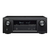
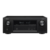
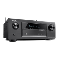
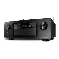
| Product color | Black |
| Audio decoders | Dolby TrueHD, DTS 96/24, DTS Neo:X, DTS-ES, DTS-HD Master Audio |
| Power consumption (standby) | 0.1 W |
| Power consumption (typical) | 670 W |
| Depth | 389 mm |
|---|---|
| Width | 434 mm |
| Height | 167 mm |
| Weight | 12600 g |