1.4. Error display
See the table below for descriptions of displayed errors and countermeasures for these.
Display order is
q
,
w
,
e
,
r
,
t
,
y
,
u
.
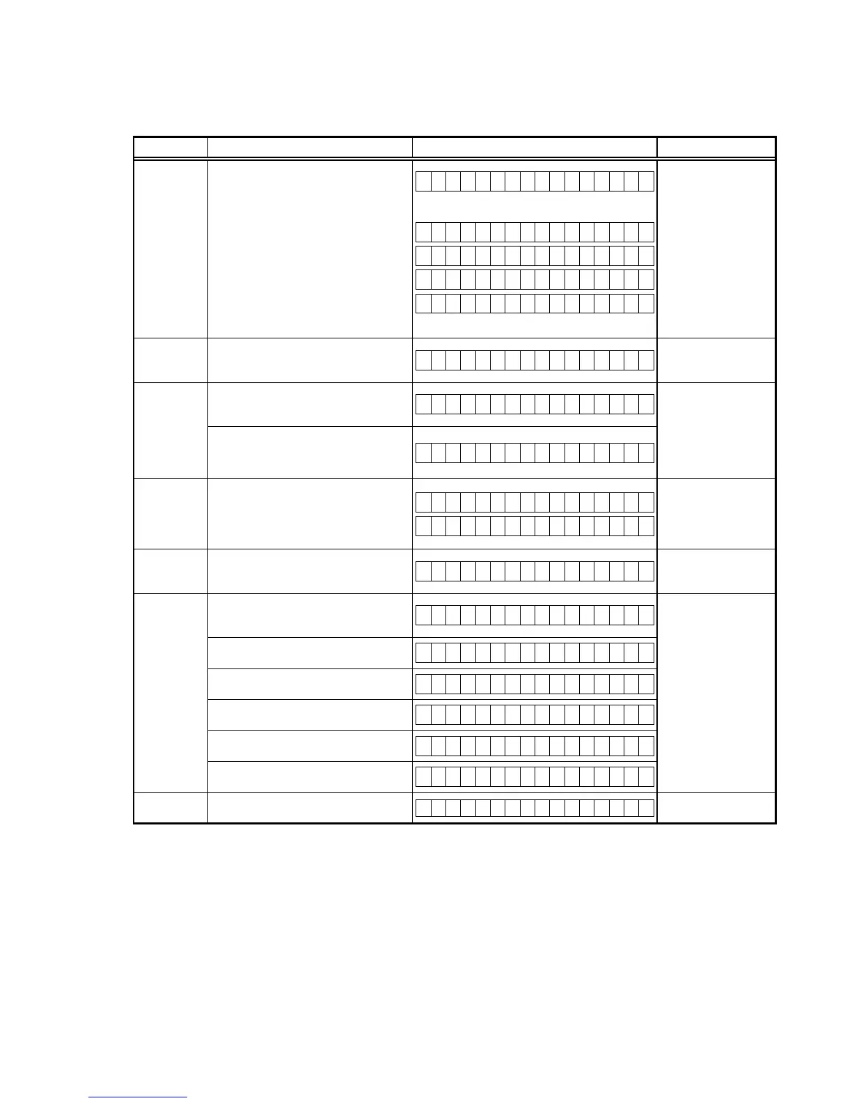
q
Firm Check
NG
The model name, brand name and region
information written in the rmware are
compared to the region settings in the
PCB.This error is displayed if the informa-
tion does not match.
" ▲ " is displayed as the rst character
if the rmware is not correct (see right
section of table).
F I R M E R R O R
–
M a i n : * * . * *
–
D S P 1 : * * . * *
–
A u d i o P L D : * * . * *
–
G U I : * * * * * * * *
• Check the resistor for
setting region(R1589 /
R1590, DIGITAL PCB).
• Write the rmware for
the correct region.
w
SUB μ -COM
NG
There is not a reply from SUBμ-COM.
S U B E R R O R 0 1
• Check the SUB(IC171)
and surrounding cir-
cuits.
e
IP SCALER NG
An error occurs in Loopback Test of the
DDR memory to perform at initial setting
of i/p Scaler(ADV8003).
I P S C A L E R E R R 0 1
• Check the circuits
around the IP SCALER
(IC401, HDMI PCB) and
DDR2 (IC402/IC403).
If there appear to be
no problems, IC401 or
IC402/IC403 is faulty.
In initial setting of i/p Scaler ( ADV8003 ),
there is not the reply of the Loopback Test
result of the DDR memory .
I P S C A L E R E R R 0 2
r
GUI Serial
Flash NG
In initial setting of i/p Scaler ( ADV8003 ),
there is not the reply of the Loopback Test
result of the DDR memory .
" ▼ " is displayed as the rst character of
the GUI rmware version
G U I V E R . E R R O R
•
G U I : * * * * * * * *
• Check the rmware
version.
t
DIR NG
This error is displayed if there is no re-
sponse from the DIR.
D I R E R R O R 0 1
• Check the DIR (IC202,
DIGITAL PCB) and
surrounding circuits.
y
DSP NG
The DSP
*
FLAG0 port does not enter "
Hi
"
status even after executing a DSP reset
during a DSP code boot.
D S P * E R R O R 0 1
• Check the DSP (IC251,
IC261, IC271, IC281
DIGITAL PCB) and
surrounding circuits.
The DSP
*
FLAG0 port does not enter "
Hi
"
status before issuing a DSP command.
D S P * E R R O R 0 2
ACK="
Hi
" does not occur during DSP
*
data reading, even when WRITE="
Lo
".
D S P * E R R O R 0 3
ACK="
Lo
" does not occur during DSP
*
data reading, even when REQ="
Lo
".
D S P * E R R O R 0 4
ACK="
Hi
" does not occur during DSP
*
data writing, even when WRITE="
Hi
".
D S P * E R R O R 0 5
ACK="
Lo
" does not occur during DSP
*
data writing, even when REQ="
Lo
".
D S P * E R R O R 0 6
u
EEPROM NG
An error occurred in a checksum of the
EEPROM(*** is a block address number).
E 2 P R O M E R R * * *
21
 Loading...