NJU72751V (INPUT : IC871)
Block Diagram
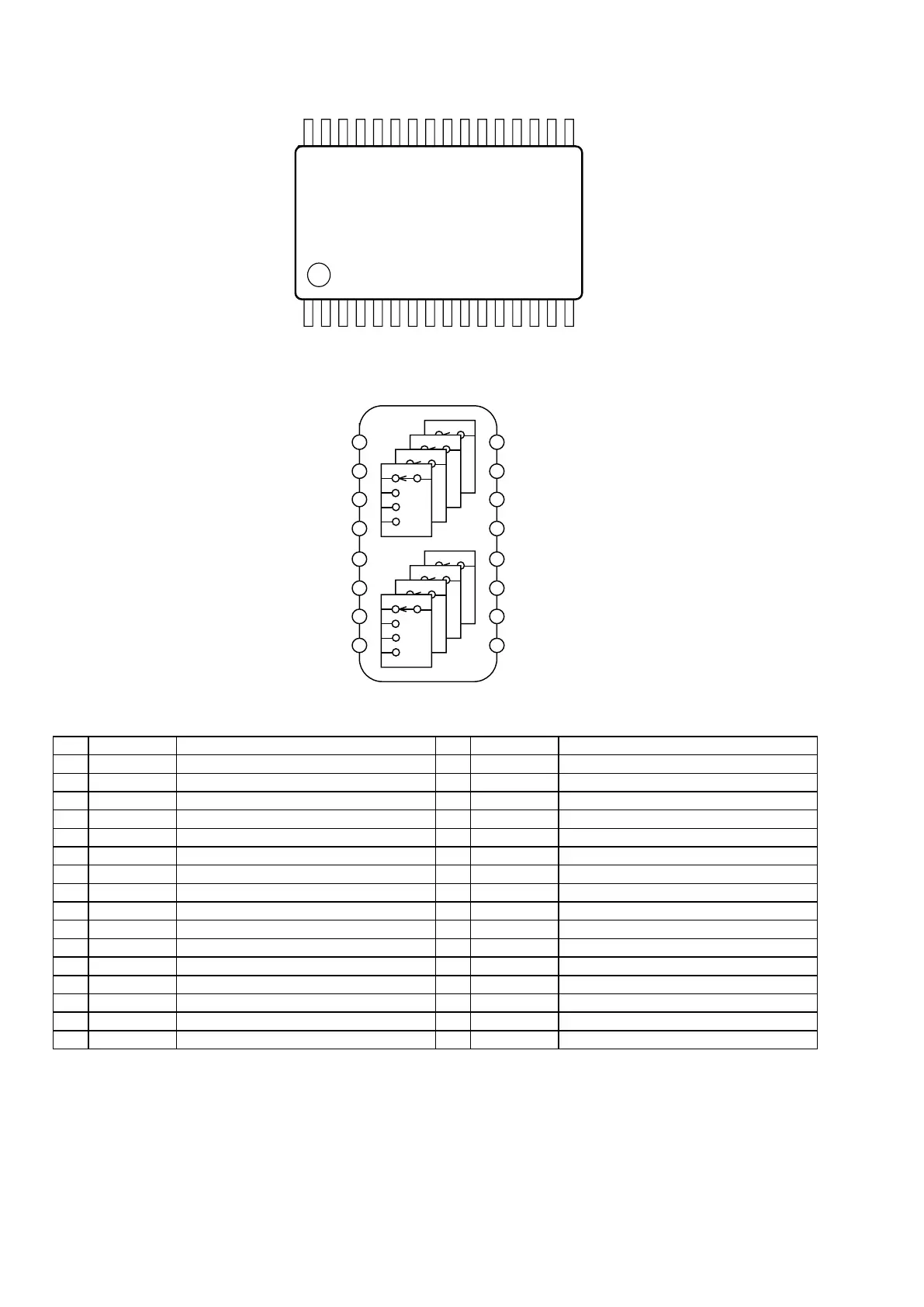
Pin Assignment
No. Symbol Function No Symbol Function
1 V+ Power supply (+) 17 CLOCK Clock signal Input terminal
2 ADR0 Chip address setting terminal 0 18 NC No connect
3 InA1 Ach Input terminal 1 19 OutB4 Bch Output terminal 4
4 InB1 Bch Input terminal 1 20 OutA4 Ach Output terminal 4
5 NC No connect 21 NC No connect
6 InA2 Ach Input terminal 2 22 OutB3 Bch Output terminal 3
7 InB2 Bch Input terminal 2 23 OutA3 Ach Output terminal 3
8 NC No connect 24 REF_B Bch Reference Voltage terminal
9 NC No connect 25 REF_A Ach Reference Voltage terminal
10 InA3 Ach Input terminal 3 26 OutB2 Bch Output terminal 2
11 InB3 Bch Input terminal 3 27 OutA2 Ach Output terminal 2
12 NC No connect 28 NC No connect
13 InA4 Ach Input terminal 4 29 OutB1 Bch Output terminal 1
14 InB4 Bch Input terminal 4 30 OutA1 Ach Output terminal 1
15 REF Digital block reference voltage terminal 31 ADR1 Chip address setting terminal 1
16 DATA Control data signal Input terminal 32 V- Power supply (-)
1
-2-
PIN CONFIGURATION
No. Symbol Function Symbol Function
1 V+
Power supply (+)
17 CLOCK
Clock signal Input terminal
2 ADR0
Chip address setting terminal 0
18 NC
No connect
3 InA1
Ach Input terminal 1
19 OutB4
Bch Output terminal 4
4 InB1
Bch Input terminal 1
20 OutA4
Ach Output terminal 4
5 NC
No connect
21 NC
No connect
6 InA2
Ach Input terminal 2
22 OutB3
Bch Output terminal 3
7 InB2
Bch Input terminal 2
23 OutA3
Ach Output terminal 3
8 NC
No connect
24 REF_B
Bch Reference Voltage terminal
9 NC
No connect
25 REF_A
Ach Reference Voltage terminal
10 InA3
Ach Input terminal 3
26 OutB2
Bch Output terminal 2
11 InB3
Bch Input terminal 3
27 OutA2
Ach Output terminal 2
12 NC
No connect
28 NC
No connect
13 InA4
Ach Input terminal 4
29 OutB1
Bch Output terminal 1
14 InB4
Bch Input terminal 4
30 OutA1
Ach Output terminal 1
15 REF
Digital block reference voltage terminal
31 ADR1
Chip address setting terminal 1
16 DATA
Control data signal Input terminal
32 V-
Power supply (-)
1 16
17
32
1
-1-
Ver.1.8E
4-INPUT / 4-OUTPUT DUAL ANALOG SWITCH
GENERAL DESCRIPTION PACKAGE OUTLINE
The NJU72751 is a 4-input / 4-output dual analog switch.
Functions are controlled via two-wired serial bus. A-channel
switches and B-channel switches are controlled independently.
The NJU72751 is well-suited for multi-channel audio systems
such as AV amplifiers, DVD receivers and others.
FEATURES
Operating Voltage ±4.5 to ±7.5V
2-wired Serial BUS Control
Selectable 2-Chip Address Available for using four chips on same serial bus line
ON Resistance 15 typ.
Low Distortion 0.0004% typ. (V
IN
=1Vrms)
CMOS Technology
Package Outline SSOP32
BLOCK DIAGRAM
InA1 OutA1
InA2 OutA2
InA3 OutA3
InA4 OutA4
InB1 OutB1
InB2 OutB2
InB3 OutB3
InB4 OutB4
180
 Loading...